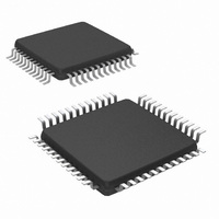
NS16C2552TVS/NOPB National Semiconductor, NS16C2552TVS/NOPB Datasheet - Page 27

NS16C2552TVS/NOPB
Manufacturer Part Number
NS16C2552TVS/NOPB
Description
IC UART DUAL 16BYTE 48-TQFP
Manufacturer
National Semiconductor
Datasheet
1.NS16C2552TVAXNOPB.pdf
(44 pages)
Specifications of NS16C2552TVS/NOPB
Features
Programmable
Number Of Channels
2, DUART
Fifo's
16 Byte
Voltage - Supply
2.97 V ~ 5.5 V
With Auto Flow Control
Yes
With Irda Encoder/decoder
Yes
With Modem Control
Yes
Mounting Type
Surface Mount
Package / Case
48-VFQFP
Lead Free Status / RoHS Status
Lead free / RoHS Compliant
Other names
NS16C2552TVS
Available stocks
Company
Part Number
Manufacturer
Quantity
Price
Company:
Part Number:
NS16C2552TVS/NOPB
Manufacturer:
Texas Instruments
Quantity:
10 000
The capacitors C1 and C2 are used to adjust the load capac-
itance on these pins. The total load capacitance (C1, C2 and
crystal)
NS16C2552/2752 to function properly. The parallel resistor
Rp and load resistor Rs are recommended by some crystal
vendors. Refer to the vendor’s crystal datasheet for details.
Since each channel has a separate programmable clock di-
vider, each channel can have a different baud rate.
The oscillator provides clock to the internal data transmission
circuitry, writing and reading from the parallel bus is not af-
fected by the oscillator frequency. For circuits not using the
external crystal, the clock input is XIN (Figure 3.)
7.2 RESET
The NS16C2552/2752 has an on-chip power-on reset that
can accommodate a slow risetime power supply. The power-
on reset has a circuit that holds the device in reset state for
2
24MHz, the reset time will be 2
external active high reset can also be applied. The default
output state of the device is listed in Table 26.
7.3 RECEIVER OPERATION
Each serial channel consists of an 8-bit Receive Shift Register
(RSR) and a 16 (or 64) -byte by 11-bit wide Receive FIFO.
The RSR contains a 8-bit Receive Buffer Register (RBR) that
is part of the Receive FIFO. The 11-bit wide FIFO contains an
8-bit data field and a 3-bit error flag field. The RSR uses 16X
clock as timing source. (Figure 4.)
23
SOUT1, SOUT2
OUT2
RTS1, RTS2
DTR1, DTR2
INTR1, INTR2
TXRDY1, TXRDY2
XIN clock cycles. For example, if the crystal frequency is
must
TABLE 26. Output State After Reset
Output
FIGURE 3. Clock Input Circuitry
be
within
a
23
X 1/(24 X 10
certain
Reset State
Logic 1
Logic 1
Logic 1
Logic 1
Logic 0
Logic 0
20204805
range
6
) = 349ms. An
for
the
27
The RSR operation is described as follows:
1.
2.
3.
7.3.1 Receive in FIFO Mode
Interrupt Mode
In the FIFO mode, FCR[0]=1, RBR can be configured to gen-
erate an interrupt after the FIFO pointer reaches a trigger
threshold. The interrupt causes CPU host to fetch the Rx
character in the FIFO in a burst mode and the transfer number
is set by the trigger level. The interrupt is cleared as soon as
the number of bytes in the Rx FIFO drops below the trigger
level. The Rx FIFO continues to receive new characters, and
the interrupt is re-asserted when the character reaches the
trigger threshold.
To ensure the data is delivered to the host, a receive data
ready time-out interrupt IIR[3] is generated when RBR data is
not fetched by the host in 4-word length long (defined in LCR
[1:0]) plus 12 bit-time. The RBR interrupt is enabled through
IER[0]. This is equivalent of 3.6 to 4.7 frame-time.
The maximum time between a received character and a time-
out interrupt will be 147 ms at 300 baud with an 8-bit receive
word.
Character delay time is calculated by using the BAUDOUT
signal as a clock signal. This makes the delay proportional to
the baud rate.
Time-out interrupt is cleared and the timer is reset when the
CPU reads one character from the Receive FIFO. When the
At the falling edge of the start bit, an internal timer starts
counting at 16X clock. At 8th 16X clock, approximately
the middle of the start bit, the logic level is sampled. If a
logic 0 is detected the start bit is validated.
The validation logic continues to detect the remaining
data bits and stop bit to ensure the correct framing. If an
error is detected, it is reported in LSR[4:2].
The data frame is then loaded into the RBR and the
Receive FIFO pointer is incremented. The error tags are
updated to reflect the status of the character data in RBR.
The data ready bit (LSR[0]) is set as soon as a character
is transferred from the shift register to the Receive FIFO.
It is reset when the Receive FIFO is empty.
FIGURE 4. Rx FIFO Mode
www.national.com
20204806


