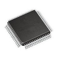
SI3232-G-GQ Silicon Laboratories Inc, SI3232-G-GQ Datasheet - Page 52

SI3232-G-GQ
Manufacturer Part Number
SI3232-G-GQ
Description
IC SLIC PROG DUAL-CH 64TQFP
Manufacturer
Silicon Laboratories Inc
Datasheet
1.SI3232-FQ.pdf
(128 pages)
Specifications of SI3232-G-GQ
Function
Subscriber Line Interface Concept (SLIC)
Interface
ISDN
Number Of Circuits
2
Voltage - Supply
3.13 V ~ 3.47 V
Current - Supply
28mA
Power (watts)
280mW
Operating Temperature
-40°C ~ 85°C
Mounting Type
Surface Mount
Package / Case
*
Product
Telecom
Lead Free Status / RoHS Status
Lead free / RoHS Compliant
Available stocks
Company
Part Number
Manufacturer
Quantity
Price
Company:
Part Number:
SI3232-G-GQ
Manufacturer:
Silicon Laboratories Inc
Quantity:
10 000
Company:
Part Number:
SI3232-G-GQR
Manufacturer:
Silicon Laboratories Inc
Quantity:
10 000
Si3232
4.17. Si3232 RAM and Register Space
The Si3232 is a highly-programmable telephone
linecard solution that uses internal registers and RAM to
program operational parameters and modes. The
Register Summary and RAM Summary are compressed
listings for single-entry quick reference. The Register
Descriptions and RAM Descriptions give detailed
information of each register or RAM location’s bits.
All RAM locations are cleared upon a hardware reset.
All RAM locations that are listed as “INIT” must be
initialized to a meaningful value for proper functionality.
Bit 4 of the MSTRSTAT register indicates the clearing
process is finished. This bit should be checked before
initializing the RAM space.
Accessing register and RAM space is performed
through the SPI. Register space is accessed by using
the standard three-byte access as described in the next
section. Bit 5 of the control byte specifies register
access when set to a 1. All register space is comprised
of 8-bit data.
4.17.1. RAM Access by Pipeline
Ram space can be accessed by two different methods.
One method is a pipeline method that employs a 4-byte
access plus a RAM status check. The control byte for
the pipeline method has bit 6 cleared to 0 to indicate a
RAM access. The control byte is followed by the RAM
address byte, then the two data bytes.
Reading RAM in the pipeline method requires “priming”
the data. First, check for register RAMSTAT, bit 0, to
indicate the previous access is complete and RAM is
ready (0). Then, perform the 4-byte RAM access. The
first read will yield unusable data. The data read on the
subsequent read access is the data for the previous
address read. A final address read yields the last
previously-requested data. The RAM-ready information
(RAMSTAT) must be read before every RAM access.
To write a RAM location, check for register RAMSTAT,
bit 0, to indicate the previous access is complete and
RAM is ready (0). Then, write the RAM address and
data in the 4-byte method. A write to RAM location
requires “priming” the data with subsequent accesses.
4.17.2. RAM Access by Register
An alternative method to access RAM space utilizes
three registers in sequence and monitors RAMSTAT
register, bit 0. These three registers are RAMADDR,
RAMDATLO, and RAMDATHI.
To read a RAM location in the Si3232, check for register
RAMSTAT (bit 0) to indicate the previous access is
complete and RAM is ready (0). Then, write the RAM
address to RAMADDR. Wait until RAMSTAT (bit 0) is a
1; then, the 16 bits of data can be read from the
52
Preliminary Rev. 0.96
RAMDATLO and RAMDATHI registers.
To write a RAM location in the Si3232, check for register
RAMSTAT (bit 0) to indicate the previous access is
completed and RAM is ready (0); then, write the 16 bits
of RAM data to the RAMDATLO, RAMDATHI. Finally,
write the RAM address to the RAMADDR register.
4.17.3. Chip Select
For register or RAM space access, there are three ways
to use chip select: byte length, 16-bit length, and access
duration length. The byte length method releases chip
select after every 8 bits of communication with the
Si3232. The time between chip select assertions must
be at least 220 ns.
The 16-bit length chip select method is similar to the
byte
communicated with the Si3232. This means that Si3232
communication consists of a control byte, address byte
for one 16-bit access, and two data bytes for a second
16-bit access.
In a single data byte communication (control byte,
address byte, data byte), the data byte should be
loaded into either the high byte or both bytes of the
second 16-bit access for a write. The 8-bit data exists in
the high and low byte of a 16-bit access for a read. The
time between chip select assertion must be at least
220 ns.
Access duration length allows chip select to be pulled
low for the length of a number of Si3232 accesses.
There are two very specific rules for this type of
communication. One rule is that the SCLK must be of a
frequency that is less than 1/2x220 ns (<2.25 MHz).
The second rule is that access must be done in a 16-bit
modulus. This 16-bit modulus follows the same rules as
described above for 16-bit length access where 8-bit
data is concerned.
4.17.4. Protected Register Bits
The Si3232 has protected register bits that are meant to
retain the integrity of the Si3232 circuit in the event of
unintentional software register access. To access the
user-protected bits, write the following sequence of data
bytes to register address 87 (0x57):
0x02
0x10
0x12
0x00
Following the modification of any protected bit, the
same sequence should be immediately written to place
these bits into their protected state.
Protected bits exist in registers SBIAS and THERM.
length
method
except
that
16-bits
are


