SI3200-GS Silicon Laboratories Inc, SI3200-GS Datasheet - Page 68

SI3200-GS
Manufacturer Part Number
SI3200-GS
Description
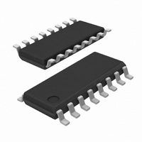
IC LINEFEED INTRFC 100V 16SOIC
Manufacturer
Silicon Laboratories Inc
Series
ProSLIC®r
Specifications of SI3200-GS
Function
Subscriber Line Interface Concept (SLIC), CODEC
Interface
GCI, PCM, SPI
Number Of Circuits
2
Voltage - Supply
3.3V, 5V
Current - Supply
110µA
Power (watts)
941mW
Operating Temperature
-40°C ~ 85°C
Mounting Type
Surface Mount
Package / Case
16-SOIC (3.9mm Width)
Includes
Battery Switching, BORSCHT Functions, DTMF Generation and Decoding, FSK Tone Generation, Modem and Fax Tone Detection
Lead Free Status / RoHS Status
Lead free / RoHS Compliant
Lead Free Status / RoHS Status
Lead free / RoHS Compliant, Lead free / RoHS Compliant
Available stocks
Company
Part Number
Manufacturer
Quantity
Price
Company:
Part Number:
SI3200-GS
Manufacturer:
SILICON
Quantity:
1
Part Number:
SI3200-GS
Manufacturer:
SILICON LABS/芯科
Quantity:
20 000
Company:
Part Number:
SI3200-GSR
Manufacturer:
SILICON
Quantity:
12 000
Si3220/Si3225
Interrupt Logic
The Dual ProSLIC devices are capable of generating
interrupts for the following events:
The interface to the interrupt logic consists of six
registers. Four interrupt status registers (IRQ0–IRQ3)
contain 1 bit for each of the above interrupt functions.
These bits are set when an interrupt is pending for the
associated resource. Three interrupt mask registers
(IRQEN1–IRQEN3) also contain 1 bit for each interrupt
function. For interrupt mask registers, the bits are active
high. Refer to the appropriate functional description text
for operational details of the interrupt functions.
When a resource reaches an interrupt condition, it
signals an interrupt to the interrupt control block. The
68
Loop current/ring ground detected
Ring trip detected
Ground Key detected
Power alarm
DTMF digit detected
Active timer 1 expired
Inactive timer 1 expired
Active timer 2 expired
Inactive timer 2 expired
Ringing active timer expired
Ringing inactive timer expired
Pulse metering active timer expired
Pulse metering inactive timer expired
RAM address access complete
Receive path modem tone detected
Transmit path modem tone detected
PCLK
PFD
T
settle
RESET
=
-------------- -
f
PCLK
64
Figure 40. PLL Frequency Synthesizer
PLL_MULT
DIV M
Rev. 1.0
Note: Therefore, the RESET pin must be held low during
interrupt control block sets the associated bit in the
interrupt status register if the mask bit for that interrupt
is set. The INT pin is a NOR of the bits of the interrupt
status registers. Therefore, if a bit in the interrupt status
registers is asserted, IRQ asserts low. Upon receiving
the interrupt, the interrupt handler should read interrupt
status registers to determine which resource requests
service. All interrupt bits in the interrupt status registers
IRQ0–IRQ3 are cleared following a register read
operation. If the interrupt status registers are non-zero,
the INT pin remains asserted.
SPI Control Interface
The control interface to the Dual ProSLIC devices is a
4-wire SPI bus modeled after microcontroller and serial
peripheral devices. The interface consists of a clock,
SCLK, chip select, CS, serial data input, SDI, and serial
data output, SDO. In addition, the Dual ProSLIC devices
include a serial data through output (SDI_THRU) to
support daisy-chain operation of up to eight devices (up
to sixteen channels). Figure 41 illustrates the daisy-
chain connections. Note that the SDITHRU pin of the
last device in the chain must not be connected to
ground (SDITHRU = 0 indicated GCI mode). The device
operates with both 8-bit and 16-bit SPI controllers. Each
SPI operation consists of a control byte, an address
byte (of which only the seven LSBs are used internally),
and either one or two data bytes depending on the width
of the controller and whether the access is to an 8-bit
register or 16-bit RAM address. Bytes are always
transmitted MSB first. The variations of usage on this
four-wire interface are as follows:
Continuous clocking . During continuous clocking,
the data transfers are controlled by the assertion of
powerup and should only be released when both
PCLK and FSYNC signals are known to be stable.
VCO
÷2
÷2
28.672 MHz


