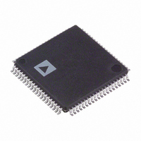
ADV3000ASTZ-RL Analog Devices Inc, ADV3000ASTZ-RL Datasheet - Page 25

ADV3000ASTZ-RL
Manufacturer Part Number
ADV3000ASTZ-RL
Description
IC HDMI/DVI SWITCH 3.1 80LQFP
Manufacturer
Analog Devices Inc
Datasheet
1.ADV3000ASTZ.pdf
(28 pages)
Specifications of ADV3000ASTZ-RL
Function
Switch
Circuit
1 x 3:1
Voltage Supply Source
Single Supply
Voltage - Supply, Single/dual (±)
3 V ~ 3.6 V
Current - Supply
110mA
Operating Temperature
-40°C ~ 85°C
Mounting Type
Surface Mount
Package / Case
80-LQFP
Lead Free Status / RoHS Status
Lead free / RoHS Compliant
Power Supply Bypassing
The ADV3000 requires minimal supply bypassing. When
powering the supplies individually, place a 0.01 μF capacitor
between each 3.3 V supply pin (AVCC, DVCC, VTTI, and VTTO)
and ground to filter out supply noise. Generally, bypass capacitors
should be placed near the power pins and should connect directly
to the relevant supplies (without long intervening traces). For
example, to improve the parasitic inductance of the power supply
decoupling capacitors, minimize the trace length between
capacitor landing pads and the vias as shown in Figure 34.
In applications where the ADV3000 is powered by a single 3.3 V
supply, it is recommended to use two reference supply planes
Figure 34. Recommended Pad Outline for Bypass Capacitors
RECOMMENDED
NOT RECOMMENDED
EXTRA ADDED INDUCTANCE
Rev. 0 | Page 25 of 28
and bypass the 3.3 V reference plane to the ground reference
plane with one 220 pF, one 1000 pF, two 0.01 μF, and one 4.7 μF
capacitors. The capacitors should via down directly to the
supply planes and be placed within a few centimeters of the
ADV3000. The AMUXVCC supply does not require additional
bypassing. This bypassing scheme is illustrated in Figure 35.
Figure 35. Example Placement of Power Supply Decoupling Capacitors
AUXILIARY LINES
TMDS TRACES
Around the ADV3000
ADV3000
DECOUPLING
CAPACITORS
ADV3000


