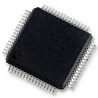
AD7609BSTZ Analog Devices Inc, AD7609BSTZ Datasheet - Page 7

AD7609BSTZ
Manufacturer Part Number
AD7609BSTZ
Description
58T8900
Manufacturer
Analog Devices Inc
Datasheet
1.AD7609BSTZ.pdf
(36 pages)
Specifications of AD7609BSTZ
Resolution (bits)
18bit
Sampling Rate
250kSPS
Input Channel Type
Differential
Data Interface
Serial, SPI
Supply Voltage Range - Analog
4.75V To 5.25V
Rohs Compliant
Yes
Available stocks
Company
Part Number
Manufacturer
Quantity
Price
Company:
Part Number:
AD7609BSTZ
Manufacturer:
ADI
Quantity:
433
Company:
Part Number:
AD7609BSTZ
Manufacturer:
ADI
Quantity:
250
Company:
Part Number:
AD7609BSTZ
Manufacturer:
Analog Devices Inc
Quantity:
10 000
Part Number:
AD7609BSTZ
Manufacturer:
ADI/亚德诺
Quantity:
20 000
Company:
Part Number:
AD7609BSTZ-RL
Manufacturer:
Analog Devices Inc
Quantity:
10 000
TIMING SPECIFICATIONS
AV
unless otherwise noted.
Table 3.
Parameter
PARALLEL/SERIAL/BYTE MODE
PARALLEL READ OPERATION
t
t
t
t
t
t
t
t
t
t
t
t
t
t
t
t
t
t
t
CC
CYCLE
CONV
WAKE-UP STANDBY
WAKE-UP SHUTDOWN
RESET
OS_SETUP
OS_HOLD
1
2
3
4
5
6
7
8
9
10
11
12
2
Internal Reference
External Reference
= 4.75 V to 5.25 V, V
1
DRIVE
= 2.3 V to 5.25 V, V
Min
3.45
7.87
16.05
33
66
133
257
50
20
20
25
25
0
25
0
0
19
24
30
37
15
22
Limit at T
Typ
5
4
MIN
, T
MAX
Max
5
10.1
11.5
4.15
9.1
18.8
39
78
158
315
100
30
13
45
0.5
25
REF
= 2.5 V external reference/ internal reference, T
Unit
μs
μs
μs
μs
μs
μs
μs
μs
μs
μs
μs
μs
ms
ms
ns
ns
ns
ns
ns
ns
ns
ms
ns
ns
ns
ns
ns
ns
ns
ns
ns
ns
Rev. 0 | Page 7 of 36
Description
1/throughput rate
Parallel mode, reading during; or after conversion V
serial mode: V
and D
Parallel mode reading after conversion V
Serial mode reading after conversion; V
Serial mode reading after a conversion; V
Conversion time
Oversampling off
Oversampling by 2
Oversampling by 4
Oversampling by 8
Oversampling by 16
Oversampling by 32
Oversampling by 64
STBY rising edge to CONVST x rising edge; power-up time from standby mode
STBY rising edge to CONVST x rising edge; power-up time from
shutdown mode
STBY rising edge to CONVST x rising edge; power-up time from
shutdown mode
RESET high pulse width
BUSY to OS x pin setup time
BUSY to OS x pin hold time
CONVST x high to BUSY high
Minimum CONVST x low pulse
Minimum CONVST x high pulse
BUSY falling edge to CS falling edge setup time
Maximum delay allowed between CONVST A, CONVST B rising edges
Maximum time between last CS rising edge and BUSY falling edge
Minimum delay between RESET low to CONVST x high
CS to RD setup time
CS to RD hold time
RD low pulse width
V
V
V
V
RD high pulse width
CS high pulse width (see
DRIVE
DRIVE
DRIVE
DRIVE
above 4.75 V
above 3.3 V
above 2.7 V
above 2.3 V
OUT
B lines
DRIVE
= 3.3 V to 5.25 V, reading during a conversion using D
Figure 5 CS and RD linked
);
DRIVE
A
DRIVE
DRIVE
= T
= 2.7 V, D
= 2.3 V, D
MIN
= 2.3 V
to T
DRIVE
OUT
MAX
OUT
A and D
A and D
= 2.7 V to 5.25 V; or
,
OUT
OUT
AD7609
B lines
B lines
OUT
A


