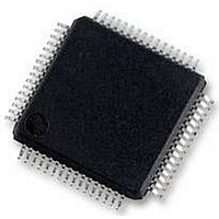
AD7609BSTZ Analog Devices Inc, AD7609BSTZ Datasheet - Page 24

AD7609BSTZ
Manufacturer Part Number
AD7609BSTZ
Description
58T8900
Manufacturer
Analog Devices Inc
Datasheet
1.AD7609BSTZ.pdf
(36 pages)
Specifications of AD7609BSTZ
Resolution (bits)
18bit
Sampling Rate
250kSPS
Input Channel Type
Differential
Data Interface
Serial, SPI
Supply Voltage Range - Analog
4.75V To 5.25V
Rohs Compliant
Yes
Available stocks
Company
Part Number
Manufacturer
Quantity
Price
Company:
Part Number:
AD7609BSTZ
Manufacturer:
ADI
Quantity:
433
Company:
Part Number:
AD7609BSTZ
Manufacturer:
ADI
Quantity:
250
Company:
Part Number:
AD7609BSTZ
Manufacturer:
Analog Devices Inc
Quantity:
10 000
Part Number:
AD7609BSTZ
Manufacturer:
ADI/亚德诺
Quantity:
20 000
Company:
Part Number:
AD7609BSTZ-RL
Manufacturer:
Analog Devices Inc
Quantity:
10 000
AD7609
TYPICAL CONNECTION DIAGRAM
Figure 41 shows the typical connection diagram for the
AD7609. There are four AV
can be tied together and decoupled using a 100 nF capacitor at
each supply pin and a 10 μF capacitor at the supply source. The
AD7609
applied reference. In this configuration, the
ured to operate with the internal reference. When using a single
AD7609
be decoupled with a 10 μF capacitor. In an application with
multiple
section. The REFCAPA and REFCAPB pins are shorted together
and decoupled with a 10 μF ceramic capacitor.
The V
cessor. The voltage on V
output logic signals. For layout, decoupling, and grounding
hints, see the Layout Guidelines section.
After supplies are applied to the AD7609, a reset should be
applied to the
correct mode of operation.
DRIVE
AD7609
can operate with the internal reference or an externally
device on the board, the REFIN/REFOUT pin should
supply is connected to the same supply as the pro-
AD7609
devices, see the Internal/External Reference
to ensure that it is configured for the
DRIVE
ANALOG INPUT PAIRS
EIGHT DIFFERENTIAL
CC
controls the voltage value of the
supply pins on the part that
1
2
DECOUPLING SHOWN ON THE AV
DECOUPLING CAPACITOR CAN BE SHARED BETWEEN AV
DECOUPLING SHOWN ON THE REGCAP PIN APPLIES TO EACH REGCAP PIN (PIN 36, PIN 39).
10µF
+
AD7609
10µF
REFIN/REFOUT
REFCAPA
REFCAPB
REFGND
V1+
V1–
V2+
V2–
V3+
V3–
V4+
V4–
V5+
V5–
V6+
V6–
V7+
V7–
V8+
V8–
+
Figure 41. Typical Connection Diagram
is config-
CC
PIN APPLIES TO EACH AV
Rev. 0 | Page 24 of 36
1µF
AD7609
REGCAP
AGND
100nF
ANALOG SUPPLY
2
VOLTAGE 5V
POWER-DOWN MODES
There are two power-down modes available on the AD7609.
The STBY pin controls whether the
or one of the two power-down modes. The two power-down
modes available are standby mode and shutdown mode. The
power-down mode is selected through the state of the RANGE
pin when the
required to choose the desired power-down mode. When the
AD7609
8 mA maximum and power-up time is approximately 100 μs
because the capacitor on the REFCAPA/REFCAPB pins must
charge up. In standby mode, the on-chip reference and
regulators remain powered up and the amplifiers and ADC core
are powered down. When the
mode, the current consumption is 11 μA maximum and power
up time is about 13 ms. In shutdown mode, all circuitry
is powered down. When the
shutdown mode, a reset signal must be applied to the
after the required power-up time has elapsed.
Table 8. Power-Down Mode Selection
Power-Down Mode
Standby
Shutdown
AV
PAR/SER SEL
DB0 TO DB15
CONVST A, B
CC
REF SELECT
CC
PIN 37 AND PIN 38.
CC
RANGE
RESET
V
is placed in standby mode, the current consumption is
BUSY
PIN (PIN 1, PIN 37, PIN 38, PIN 48).
1
STBY
OS 2
OS 1
OS 0
DRIVE
RD
CS
STBY pin is low.
DIGITAL SUPPLY
VOLTAGE +2.3V TO +5V
100nF
INTERFACE
PARALLEL
OVERSAMPLING
V
DRIVE
V
DRIVE
AD7609
AD7609
Table 8
AD7609
STBY
0
0
is powered up from
shows the configurations
is placed in shutdown
is in normal mode
RANGE
1
0
AD7609


