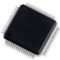
AD7609BSTZ Analog Devices Inc, AD7609BSTZ Datasheet - Page 14

AD7609BSTZ
Manufacturer Part Number
AD7609BSTZ
Description
58T8900
Manufacturer
Analog Devices Inc
Datasheet
1.AD7609BSTZ.pdf
(36 pages)
Specifications of AD7609BSTZ
Resolution (bits)
18bit
Sampling Rate
250kSPS
Input Channel Type
Differential
Data Interface
Serial, SPI
Supply Voltage Range - Analog
4.75V To 5.25V
Rohs Compliant
Yes
Available stocks
Company
Part Number
Manufacturer
Quantity
Price
Company:
Part Number:
AD7609BSTZ
Manufacturer:
ADI
Quantity:
433
Company:
Part Number:
AD7609BSTZ
Manufacturer:
ADI
Quantity:
250
Company:
Part Number:
AD7609BSTZ
Manufacturer:
Analog Devices Inc
Quantity:
10 000
Part Number:
AD7609BSTZ
Manufacturer:
ADI/亚德诺
Quantity:
20 000
Company:
Part Number:
AD7609BSTZ-RL
Manufacturer:
Analog Devices Inc
Quantity:
10 000
AD7609
Pin No.
5, 4, 3
33
32
31 to 27
24
25
22 to 16
1
Refers to classification of pin type; P denotes power, AI denotes analog input, REF denotes reference, DI denotes digital input, DO denotes digital output.
Type
DI
DO/DI
DO/DI
DO
DO
DO
DO
1
Mnemonic
OS [2:0]
DB15
DB14
DB[13:9]
DB7/D
DB8/D
DB[6:0]
OUT
OUT
A
B
Description
Oversampling Mode Pins. Logic inputs. These inputs are used to select the oversampling ratio. OS 2 is
the MSB control bit, and OS 0 is the LSB control bit. See the Digital Filter section for additional details
on the oversampling mode of operation and Table 9 for oversampling bit decoding.
Parallel Output Data Bits, Data Bit 15. When PAR/SER SEL = 0, this pin acts as three-state parallel digital
output pin. This pin is used to output DB17 of the conversion result during the first RD pulse and DB1
of the same conversion result during the second RD pulse. When PAR/SER SEL = 1, this pin should be
tied to AGND.
Parallel Output Data Bits, Data Bit 14. When PAR/SER SEL = 0, this pin acts as three-state parallel digital
output pin. When CS and RD are low, this pin is used to output DB16 of the conversion result during
the first RD pulse and DB0 of the same conversion result during the second RD pulse. When PAR/SER
SEL = 1, this pin should be tied to AGND.
Parallel Output Data Bits, Data Bit 13 to Data Bit 9. When PAR/SER SEL = 0, these pins act as three-state
parallel digital input/output pins. When CS and RD are low, these pins are used to output DB15 to
DB11 of the conversion result during the first RD pulse and output 0 during the second RD pulse.
When PAR/SER SEL = 1, these pins should be tied to AGND.
Parallel Output Data Bit 7 (DB7)/Serial Interface Data Output Pin (D
pins acts as a three-state parallel digital input/output pin. When CS and RD are low, this pin is used to
output DB9 of the conversion result. When PAR/SER SEL = 1, this pin functions as D
serial conversion data. See the
Parallel Output Data Bit 8 (DB8)/Serial Interface Data Output Pin (D
pins acts as a three-state parallel digital input/output pin. When CS and RD are low, this pin is used to
output DB10 of the conversion result. When PAR/SER SEL = 1, this pin functions as D
serial conversion data. See the
Parallel Output Data Bits, Data Bit 6 to Data Bit 0. When PAR/SER SEL = 0, these pins act as three-state
parallel digital input/output pins. When CS and RD are low, these pins are used to output DB8 to DB2
of the conversion result during the first RD pulse and output 0 during the second RD pulse. When
PAR/SER SEL = 1, these pins should be tied to AGND.
Rev. 0 | Page 14 of 36
Conversion Control
Conversion Control
section for further details.
section for further details.
OUT
OUT
A). When PAR/SER SEL = 0, this
B). When PAR/SER SEL = 0, this
OUT
OUT
A and outputs
B and outputs


