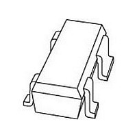
BF1101WRT NXP Semiconductors, BF1101WRT Datasheet - Page 8

BF1101WRT
Manufacturer Part Number
BF1101WRT
Description
Manufacturer
NXP Semiconductors
Datasheet
1.BF1101WRT.pdf
(15 pages)
Specifications of BF1101WRT
Application
VHF/UHF
Channel Type
N
Channel Mode
Enhancement
Continuous Drain Current
0.03A
Drain Source Voltage (max)
7V
Noise Figure (max)
2.5dB
Frequency (max)
1GHz
Package Type
CMPAK
Pin Count
3 +Tab
Input Capacitance (typ)@vds
2.2@5V@Gate 1/1.6@5V@Gate 2pF
Output Capacitance (typ)@vds
1.2@5VpF
Reverse Capacitance (typ)
0.025@5VpF
Operating Temp Range
-65C to 150C
Mounting
Surface Mount
Number Of Elements
1
Power Dissipation (max)
200mW
Screening Level
Military
Lead Free Status / Rohs Status
Compliant
NXP Semiconductors
1999 May 14
handbook, halfpage
handbook, halfpage
N-channel dual-gate MOS-FETs
V
I
V
I
D
Fig.17 Input admittance as a function of frequency;
D
DS
DS
Fig.19 Forward transfer admittance and phase as
= 12 mA; T
= 12 mA; T
(mS)
(mS)
|y fs |
y is
10
= 5 V; V
= 5 V; V
10
10
10
10
−1
1
2
1
2
10
10
typical values.
a function of frequency; typical values.
G2
G2
amb
amb
= 4 V.
= 4 V.
= 25 C.
= 25 C.
10
10
2
2
g is
b is
|y fs |
ϕ fs
f (MHz)
f (MHz)
MGS311
MGS313
10
10
3
3
−10
−10
−1
(deg)
ϕ fs
2
8
handbook, halfpage
handbook, halfpage
V
I
D
V
I
D
DS
Fig.18 Reverse transfer admittance and phase as
DS
= 12 mA; T
(mS)
(mS)
|y rs |
= 12 mA; T
y os
10
= 5 V; V
10
= 5 V; V
10
10
−1
Fig.20 Output admittance as a function of
1
BF1101; BF1101R; BF1101WR
1
2
10
10
a function of frequency; typical values.
G2
G2
amb
amb
= 4 V.
= 4 V.
frequency; typical values.
= 25 C.
= 25 C.
10
10
2
2
|y rs |
g os
b os
ϕ rs
f (MHz)
f (MHz)
Product specification
MGS314
MGS312
10
10
3
−10
−10
−1
3
(deg)
ϕ rs
2


