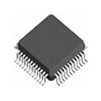
ICS8530DY IDT, Integrated Device Technology Inc, ICS8530DY Datasheet

ICS8530DY
Specifications of ICS8530DY
Available stocks
Related parts for ICS8530DY
ICS8530DY Summary of contents
Page 1
... Q9 Q6 nQ9 nQ6 Q8 Q7 nQ8 nQ7 ICS8530DY REVISION E SEPTEMBER 15, 2010 Features • Sixteen differential LVPECL output pairs • CLK, nCLK input pair • CLK, nCLK pair can accept the following differential input levels: LVPECL, LVDS, LVHSTL, HCSL, SSTL • ...
Page 2
... NOTE: Pullup and Pulldown refer to internal input resistors. See Table 2, Pin Characteristics, for typical values. Table 2. Pin Characteristics Symbol Parameter C Input Capacitance IN R Input Pullup Resistor PULLUP R Input Pulldown Resistor PULLDOWN ICS8530DY REVISION E SEPTEMBER 15, 2010 Name Type V Power CCO Output Output V Power EE Output Output ...
Page 3
... Table 4A. Power Supply DC Characteristics, V Symbol Parameter V Positive Supply Voltage CC V Output Supply Voltage CCO I Power Supply Current EE ICS8530DY REVISION E SEPTEMBER 15, 2010 LOW SKEW, 1-TO-16, DIFFERENTIAL-TO-2.5V LVPECL FANOUT BUFFER Outputs Q[0:15] nQ[0:15] Input to Output Mode LOW HIGH Differential to Differential HIGH LOW Differential to Differential ...
Page 4
... NOTE 4: Defined as skew between outputs on different devices operating at the same supply voltage, same temperature and with equal load conditions. Using the same type of inputs on each device, the outputs are measured at the differential cross points. ICS8530DY REVISION E SEPTEMBER 15, 2010 LOW SKEW, 1-TO-16, DIFFERENTIAL-TO-2.5V LVPECL FANOUT BUFFER = 3.3V ± ...
Page 5
... Qy tsk(o) Output Skew nQ[0:15] Q[0:15 PERIOD t PW odc = t PERIOD Output Duty Cycle/Pulse Width/Period ICS8530DY REVISION E SEPTEMBER 15, 2010 LOW SKEW, 1-TO-16, DIFFERENTIAL-TO-2.5V LVPECL FANOUT BUFFER SCOPE Qx nQx Differential Input Level nQx Qx nQy Qy Part-to-Part Skew nCLK CLK nQ[0:15] Q[0:15] x 100% Propagation Delay ...
Page 6
... Recommendations for Unused Output Pins Outputs: LVPECL Outputs The unused LVPECL output pair can be left floating. We recommend that there is no trace attached. Both sides of the differential output pair should either be left floating or terminated. ICS8530DY REVISION E SEPTEMBER 15, 2010 LOW SKEW, 1-TO-16, DIFFERENTIAL-TO-2.5V LVPECL FANOUT BUFFER 80 20% ...
Page 7
... This can be done in one of two ways. First, R3 and R4 in parallel should equal the transmission Figure 1. Recommended Schematic for Wiring a Differential Input to Accept Single-ended Levels ICS8530DY REVISION E SEPTEMBER 15, 2010 line impedance. For most 50Ω applications, R3 and R4 can be 100Ω ...
Page 8
... R1 50Ω *Optional – R3 and R4 can be 0Ω Figure 2E. CLK/nCLK Input Driven by a 3.3V HCSL Driver ICS8530DY REVISION E SEPTEMBER 15, 2010 LOW SKEW, 1-TO-16, DIFFERENTIAL-TO-2.5V LVPECL FANOUT BUFFER with the vendor of the driver component to confirm the driver must meet the V and termination requirements. For example in Figure 2A, the input ...
Page 9
... Figure 3A. 2.5V LVPECL Driver Termination Example V = 2.5V CC 50Ω 50Ω 2.5V LVPECL Driver Figure 3C. 2.5V LVPECL Driver Termination Example ICS8530DY REVISION E SEPTEMBER 15, 2010 level. The R3 in Figure 3B can be eliminated and the termination is shown in Figure 3C. – very close to ground 2.5V 2.5V R3 250Ω ...
Page 10
... Linear Feet per Minute Single-Layer PCB, JEDEC Standard Test Boards Multi-Layer PCB, JEDEC Standard Test Boards NOTE: Most modern PCB designs use multi-layered boards. The data in the second row pertains to most designs. ICS8530DY REVISION E SEPTEMBER 15, 2010 = 3. 3.465V, which gives worst case results ...
Page 11
... CCO_MAX [(2V – 0.7V)/50Ω] * 0.7V = 18.2mW Pd_L = [(V – (V – 2V))/R OL_MAX CCO_MAX [(2V – 1.4V)/50Ω] * 1.4V = 16.8mW Total Power Dissipation per output pair = Pd_H + Pd_L = 35mW ICS8530DY REVISION E SEPTEMBER 15, 2010 LOW SKEW, 1-TO-16, DIFFERENTIAL-TO-2.5V LVPECL FANOUT BUFFER V OUT RL 50Ω CCO = V – ...
Page 12
... Multi-Layer PCB, JEDEC Standard Test Boards NOTE: Most modern PCB designs use multi-layered boards. The data in the second row pertains to most designs. Transistor Count The transistor count for ICS8530 is: 930 ICS8530DY REVISION E SEPTEMBER 15, 2010 LOW SKEW, 1-TO-16, DIFFERENTIAL-TO-2.5V LVPECL FANOUT BUFFER θ vs. Air Flow ...
Page 13
... Basic D2 & E2 5.50 Ref. e 0.5 Basic L 0.45 0.60 θ 0° ccc Reference Document: JEDEC Publication 95, MS-026 ICS8530DY REVISION E SEPTEMBER 15, 2010 LOW SKEW, 1-TO-16, DIFFERENTIAL-TO-2.5V LVPECL FANOUT BUFFER Maximum 1.60 0.15 1.45 0.27 0.20 0.75 7° 0.08 13 ©2010 Integrated Device Technology, Inc. ...
Page 14
... IDT. IDT reserves the right to change any circuitry or specifications without notice. IDT does not authorize or warrant any IDT product for use in life support devices or critical medical instruments. ICS8530DY REVISION E SEPTEMBER 15, 2010 LOW SKEW, 1-TO-16, DIFFERENTIAL-TO-2.5V LVPECL FANOUT BUFFER ...
Page 15
... Updated Termination for LVPECL Outputs section Ordering Information Table - deleted “ICS” prefix from part/order column. Added lead-free marking. Converted datasheet format. ICS8530DY REVISION E SEPTEMBER 15, 2010 = -0.5V ± 0.165V"" from ""V = -0.5V ± 0.135V"" 4pF max. to 4pF typical. ...
Page 16
ICS8530 Data Sheet We’ve Got Your Timing Solution 6024 Silver Creek Valley Road Sales 800-345-7015 (inside USA) San Jose, California 95138 +408-284-8200 (outside USA) Fax: 408-284-2775 www.IDT.com/go/contactIDT DISCLAIMER Integrated Device Technology, Inc. (IDT) and its subsidiaries reserve the right to ...


