ICS8701CY IDT, Integrated Device Technology Inc, ICS8701CY Datasheet
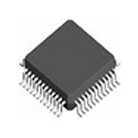
ICS8701CY

Manufacturer Part Number
ICS8701CY
Description
Manufacturer
IDT, Integrated Device Technology Inc
Type
Clock Dividerr
Datasheet

Specifications of ICS8701CY

Number Of Clock Inputs
1
Mode Of Operation
Single-Ended
Output Frequency
250MHz
Output Logic Level
LVCMOS/LVTTL
Operating Supply Voltage (min)
3.135V
Operating Supply Voltage (typ)
3.3V
Operating Supply Voltage (max)
3.465V
Package Type
TQFP
Operating Temp Range
0C to 70C
Operating Temperature Classification
Commercial
Signal Type
LVCMOS/LVTTL
Mounting
Surface Mount
Pin Count
48
Lead Free Status / Rohs Status
Not Compliant

Available stocks

Company
Part Number
Manufacturer
Quantity
Price
Part Number:
ICS8701CY
Quantity:
327
Part Number:
ICS8701CYILF
Manufacturer:
IDT, Integrated Device Technology Inc
Quantity:
10 000
Part Number:
ICS8701CYILFT
Manufacturer:
IDT, Integrated Device Technology Inc
Quantity:
10 000
Part Number:
ICS8701CYLF
Manufacturer:
IDT, Integrated Device Technology Inc
Quantity:
10 000
Part Number:
ICS8701CYLFT
Manufacturer:
IDT, Integrated Device Technology Inc
Quantity:
10 000
Part Number:
ICS8701CYT
Manufacturer:
IDT, Integrated Device Technology Inc
Quantity:
10 000
G
The ICS8701 is a low skew, ÷1, ÷2 LVCMOS/LVTTL Clock
Generator . The low impedance LVCMOS outputs are
designed to drive 50Ω series orparallel terminated
transmission lines. The effective fanout can be increased
from 20 to 40 by utilizing the ability of the outputs to drive
two series terminated lines.
The divide select inputs, DIV_SELx, control the output
frequency of each bank. The outputs can be utilized in the
÷1, ÷2 or a combination of ÷1 and ÷2 modes. The bank
enable inputs, BANK_EN0:1, support enabling and
disabling each bank of outputs individually. The master
reset input, nMR/OE, resets the internal frequency dividers
and also controls the active and high impedance states of
all outputs.
The ICS8701 is characterized at 3.3V and mixed
3.3V input supply, and 2.5V output supply operating
modes. Guaranteed bank, output and part-to-part skew
characteristics make the ICS8701 ideal for those clock
distribution applications demanding well defined
performance and repeatability.
B
8701CY
LOCK
ENERAL
BANK_EN0
BANK_EN1
DIV_SELC
DIV_SELD
DIV_SELA
DIV_SELB
nMR/OE
CLK
D
IAGRAM
D
ESCRIPTION
÷1
÷2
1
0
1
0
1
0
1
0
Bank Enable
Logic
QA0:QA4
QB0:QB4
QC0:QC4
QD0:QD4
www.idt.com
1
P
F
• Twenty LVCMOS outputs, 7Ω typical output impedance
• One LVCMOS/LVTTL clock input
• Maximum output frequency: 250MHz
• Bank enable logic allows unused banks to be disabled
• Output skew: 250ps (maximum)
• Part-to-part skew: 600ps (maximum)
• Bank skew: 200ps (maximum)
• Multiple frequency skew: 300ps (maximum)
• 3.3V or mixed 3.3V input, 2.5V output operating
• 0°C to 70°C ambient operating temperature
• Other divide values available on request
• Available in both standard and lead-free RoHS compliant
in reduced fanout applications
supply modes
packages
EATURES
IN
A
GND
GND
V
V
V
QC3
QC4
QD0
QD1
QD2
QD3
QD4
LVCMOS/LVTTL C
DDO
DDO
DDO
SSIGNMENT
1
2
3
4
5
6
7
8
9
10
11
12
48 47 46 45 44 43 42 41 40 39 38 37
13 14 15 16 17 18 19 20 21 22 23 24
7mm x 7mm x 1.4mm
ICS8701
48-Pin LQFP
Y Package
Top View
L
OW
LOCK
S
ICS8701
KEW
36
35
34
33
32
31
30
29
28
27
26
25
G
REV. E JULY 31, 2010
ENERATOR
, ÷1, ÷2
QB1
V
QB0
QA4
V
QA3
GND
QA2
GND
QA1
V
QA0
DDO
DDO
DDO

Related parts for ICS8701CY

ICS8701CY Summary of contents

Page 1

G D ENERAL ESCRIPTION The ICS8701 is a low skew, ÷1, ÷2 LVCMOS/LVTTL Clock Generator . The low impedance LVCMOS outputs are designed to drive 50Ω series orparallel terminated transmission lines. The effective fanout can be increased from 20 to ...

Page 2

ABLE IN ESCRIPTIONS ...

Page 3

ABLE IN HARACTERISTICS ...

Page 4

BSOLUTE AXIMUM ATINGS Supply Voltage Inputs Outputs Package Thermal Impedance, θ JA Storage Temperature, T STG T 4A ABLE OWER UPPLY HARACTERISTICS ...

Page 5

T 4B. LVCMOS DC C ABLE HARACTERISTICS ...

Page 6

T 5A ABLE HARACTERISTICS ...

Page 7

P ARAMETER 1.65V± DDO LVCMOS GND -1.165V±5% 3.3V C /3. ORE UTPUT OAD EST V DDO DDO sk( UTPUT KEW V DDO ...

Page 8

Driver Termination For LVCMOS Output Termination, please refer to a separate Application Note: LVCMOS Driver Termination ECOMMENDATIONS FOR NUSED I : NPUTS LVCMOS ONTROL INS All control pins have internal pull-ups or pull-downs; additional ...

Page 9

ABLE VS IR LOW ABLE FOR JA θ θ θ θ θ Single-Layer PCB, JEDEC Standard Test Boards Multi-Layer PCB, JEDEC Standard Test Boards NOTE: Most modern PCB designs use multi-layered ...

Page 10

ACKAGE UTLINE UFFIX FOR EAD ABLE ...

Page 11

ABLE RDERING NFORMATION ...

Page 12

...

Page 13

We’ve Got Your Timing Solution. 6024 Silver Creek Valley Road San Jose, CA 95138 © 2010 Integrated Device Technology, Inc. All rights reserved. Product specifications subject to change without notice. IDT, the IDT logo, ICS and HiPerClockS are trademarks of ...

Related keywords