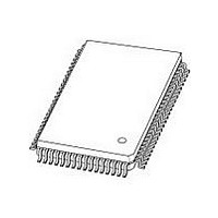
P80C557E4EFB NXP Semiconductors, P80C557E4EFB Datasheet - Page 9

P80C557E4EFB
Manufacturer Part Number
P80C557E4EFB
Description
Manufacturer
NXP Semiconductors
Datasheet
1.P80C557E4EFB.pdf
(72 pages)
Specifications of P80C557E4EFB
Cpu Family
80C
Device Core
80C51
Device Core Size
8b
Frequency (max)
16MHz
Interface Type
I2C/UART
Program Memory Type
ROMLess
Program Memory Size
Not Required
Total Internal Ram Size
1KB
# I/os (max)
40
Number Of Timers - General Purpose
3
Operating Supply Voltage (typ)
5V
Operating Supply Voltage (max)
5.5V
Operating Supply Voltage (min)
4.5V
On-chip Adc
8-chx10-bit
Instruction Set Architecture
CISC
Operating Temp Range
-40C to 85C
Operating Temperature Classification
Industrial
Mounting
Surface Mount
Pin Count
80
Package Type
PQFP
Lead Free Status / Rohs Status
Compliant
Available stocks
Company
Part Number
Manufacturer
Quantity
Price
Company:
Part Number:
P80C557E4EFB
Manufacturer:
PHILIPS
Quantity:
325
Part Number:
P80C557E4EFB
Manufacturer:
NXP/恩智浦
Quantity:
20 000
Company:
Part Number:
P80C557E4EFB/01
Manufacturer:
SAMSUNG
Quantity:
10 000
Company:
Part Number:
P80C557E4EFB/01,51
Manufacturer:
SILICON
Quantity:
459
Company:
Part Number:
P80C557E4EFB/01,51
Manufacturer:
NXP Semiconductors
Quantity:
10 000
Company:
Part Number:
P80C557E4EFB/01,55
Manufacturer:
IR
Quantity:
20
Company:
Part Number:
P80C557E4EFB/01,55
Manufacturer:
NXP Semiconductors
Quantity:
10 000
1.
Philips Semiconductors
6.2.1 Program Memory
The program memory of the P8xC557E4 consists of 32 Kbytes
ROM respectively FEEPROM (”Flash Memory”) on-chip, externally
expandable up to 64 Kbytes. If, during RESET, the EA pin was held
HIGH, the P8xC557E4 executes out of the internal program memory
unless the address exceeds 7FFFH. Locations 8000H through
0FFFFH are then fetched from the external program memory. If the
EA pin was held LOW during RESET the P8xC557E4 fetches all
instructions from the external program memory. The EA input is
latched during RESET and is don’t care after RESET.
The internal program memory content is protected, by setting a
mask programmable security bit (ROM) or by the software
programmable security byte (FEEPROM) respectively, i.e. it cannot
be read out at any time by any test mode or by any instruction in the
external program memory space. The MOVC instructions are the
only ones which have access to program code in the internal or
external program memory. The EA input is latched during RESET
and is ’don’t care’ after RESET. This implementation prevents from
reading internal program code by switching from external program
memory to internal program memory during MOVC instruction or an
instruction that handles immediate data. Table 1 lists the access to
the internal and external program memory with MOVC instructions
when the security feature has been activated.
6.2.2 Internal Data Memory
The internal data memory is divided into three physically separated
parts:
256 bytes of RAM, 768 bytes of AUX-RAM, and a 128 bytes special
function area. These can be addressed each in a different way (see
also Table 2).
– RAM 0 to 127 can be addressed directly and indirectly as in the
Table 1. Memory Access by the MOVC Instruction for Protected ROMs
NOTE:
Table 2. Internal Data Memory Map
1999 Mar 02
MOVC in internal program memory
MOVC in external program memory
LOCATION
RAM
AUX-RAM
RAM
SFR
80C51. Address pointers are R0 and R1 of the selected
registerbank.
Single-chip 8-bit microcontroller
If the security feature has not been activated, there are no restrictions for MOVC instructions.
MOVC LOCATION
128 to 255
128 to 255
0 to 127
0 to 767
ACCESS TO INTERNAL
PROGRAM MEMORY
YES
NO
9
ADDRESSED
Direct and indirect
Indirect only with MOVX
Indirect only
Direct only
P83C557E4/P80C557E4/P89C557E4
– RAM 128 to 255 can only be addressed indirectly.
– AUX-RAM 0 to 767 is also indirectly addressable as external
– The Special Function Registers (SFR) can only be addressed
– Four register banks, each 8 registers wide, occupy locations 0
Address pointers are R0 and R1 of the selected registerbank.
DATA MEMORY locations 0 to 767 via MOVX-Datapointer
instruction, unless it is disabled by setting ARD = 1.
AUX-RAM 0 to 767 is indirectly addressable via pageregister
(XRAMP) and MOVX-Ri instructions, unless it is disabled by
setting ARD = 1 (see Figure 5).
When executing from internal program memory, an access to
AUX-RAM 0 to 767 will not affect the ports P0, P2, P3.6 and P3.7.
An access to external DATA MEMORY locations higher than 767
will be performed with the MOVX @ DPTR instructions in the
same way as in the 80C51 structure, so with P0 and P2 as
data/address bus and P3.6 and P3.7 as write and read timing
signals. Note that the external DATA MEMORY cannot be
accessed with R0 and R1 as address pointer if the AUX-RAM is
enabled (ARD = 0, default).
directly in the address range from 128 to 255 (see Table 5).
through 31 in the lower RAM area. Only one of these banks may
be enabled at a time. The next 16 bytes, locations 32 through 47,
contain 128 directly addressable bit locations.The stack can be
located anywhere in the internal 256 bytes RAM.The stack depth
is only limited by the available internal RAM space of 256 bytes
(see Figure 7).
All registers except the program counter and the four register
banks reside in the Special Function Register address space.
ACCESS TO EXTERNAL
PROGRAM MEMORY
YES
YES
Product specification


