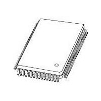
P80C557E4EFB NXP Semiconductors, P80C557E4EFB Datasheet - Page 11

P80C557E4EFB
Manufacturer Part Number
P80C557E4EFB
Description
Manufacturer
NXP Semiconductors
Datasheet
1.P80C557E4EFB.pdf
(72 pages)
Specifications of P80C557E4EFB
Cpu Family
80C
Device Core
80C51
Device Core Size
8b
Frequency (max)
16MHz
Interface Type
I2C/UART
Program Memory Type
ROMLess
Program Memory Size
Not Required
Total Internal Ram Size
1KB
# I/os (max)
40
Number Of Timers - General Purpose
3
Operating Supply Voltage (typ)
5V
Operating Supply Voltage (max)
5.5V
Operating Supply Voltage (min)
4.5V
On-chip Adc
8-chx10-bit
Instruction Set Architecture
CISC
Operating Temp Range
-40C to 85C
Operating Temperature Classification
Industrial
Mounting
Surface Mount
Pin Count
80
Package Type
PQFP
Lead Free Status / Rohs Status
Compliant
Available stocks
Company
Part Number
Manufacturer
Quantity
Price
Company:
Part Number:
P80C557E4EFB
Manufacturer:
PHILIPS
Quantity:
325
Part Number:
P80C557E4EFB
Manufacturer:
NXP/恩智浦
Quantity:
20 000
Company:
Part Number:
P80C557E4EFB/01
Manufacturer:
SAMSUNG
Quantity:
10 000
Company:
Part Number:
P80C557E4EFB/01,51
Manufacturer:
SILICON
Quantity:
459
Company:
Part Number:
P80C557E4EFB/01,51
Manufacturer:
NXP Semiconductors
Quantity:
10 000
Company:
Part Number:
P80C557E4EFB/01,55
Manufacturer:
IR
Quantity:
20
Company:
Part Number:
P80C557E4EFB/01,55
Manufacturer:
NXP Semiconductors
Quantity:
10 000
Philips Semiconductors
Table 5. Special Function Register Memory Map and Reset Values
NOTES:
%
#
X
*
6.3 Addressing
The P8xC557E4 has five methods for addressing:
The first three methods can be used for addressing destination
operands. Most instructions have a “destination/source” field that
specifies the data type, addressing methods and operands involved.
For operations other than MOVs, the destination operand is also a
source operand.
1999 Mar 02
Register
Direct
Register-Indirect
Immediate
Base-Register plus Index-Register-Indirect
LOW
Single-chip 8-bit microcontroller
A
B
C
D
E
0
1
2
3
4
5
6
7
8
9
F
=
=
=
=
Bit addressable register
Read only register
Undefined
FMCON only in P89C557E4
SP 00000111
XXXXXXXX
ADRSL0 #
00000000
00000000
00000000
00000000
00000000
00000000
00000000
00000000
00000000
TCON %
11111111
PCON
TMOD
P0 %
DPL
TH0
TH1
DPH
TL0
TL1
8
XXXXXXXX
XXXXXXXX
ADRSL1 #
S0CON %
00000000
11111111
S0BUF
P1 %
9
XXXXXXXX
XXXXXXXX
XXXXXXXX
XXXXXXXX
XXXXXXXX
ADRSL2 #
00000000
00000000
00000000
00000000
11111111
CTL0 #
CTL1 #
CTL2 #
CTL3 #
IEN0 %
CML0
CML1
CML2
P2 %
A
HIGH NIBBLE OF SFR ADDRESS
XXXXXXXX
ADRSL3 #
X0000000
11111111
IP0 %
P3 %
B
11
P83C557E4/P80C557E4/P89C557E4
Access to memory addresses is as follows:
Register in one of the four register banks through Register, Direct
or Register-Indirect addressing
1024 bytes of internal RAM through Direct or Register-Indirect
addressing.
– Bytes 0–127 of internal RAM may be addressed
– Bytes 0–767 of AUX-RAM can only be addressed indirectly via
Special Function Register through direct addressing at address
locations 128–255 (see Figure 8).
External data memory through Register-Indirect addressing
Program memory look-up tables through Base-Register plus
Index-Register-Indirect addressing
XXXXXXXX
XXXXXXXX
XXXXXXXX
XXXXXXXX
XXXXXXXX
XXXXXXXX
ADRSL4 #
00000000
00000000
00000000
00000000
directly/indirectly. Bytes 128–255 of internal RAM share their
address location with the SFRs and so may only be addressed
indirectly as data RAM.
MOVX.
TM2IR %
11111111
CTH0 #
CTH2 #
CTH3 #
CTH1 #
CMH0
CMH1
CMH2
P4 %
P5 #
C
XXXXXXXX
ADRSL5 #
S1CON %
00000000
00000000
00000000
00000000
00000000
11111000
S1STA #
ADCON
PSW %
S1ADR
S1DAT
D
XXXXXXXX
ADRSL6 #
00000000
00000000
00000000
00000000
00000000
00000000
00000000
11000000
00000000
TM2CON
CTCON
TMH2 #
ADPSS
IEN1 %
TML2 #
ACC %
STE
RTE
E
Product specification
XXXXXXXX
XXXXXX00
ADRSL7 #
000000XX
000X0000
00000000
00000000
00001101
00000000
00000000
00000000
00000000
ADRSH #
FMCON *
PLLCON
XRAMP
PWMP
PWM0
PWM1
IP1 %
B %
T3
F


