ICS87016AY IDT, Integrated Device Technology Inc, ICS87016AY Datasheet
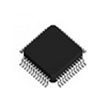
ICS87016AY

Manufacturer Part Number
ICS87016AY
Description
Manufacturer
IDT, Integrated Device Technology Inc
Type
Clock Dividerr
Datasheet

Specifications of ICS87016AY

Number Of Clock Inputs
2
Output Frequency
250MHz
Output Logic Level
LVCMOS/LVTTL
Operating Supply Voltage (min)
3.135V
Operating Supply Voltage (typ)
3.3V
Operating Supply Voltage (max)
3.465V
Package Type
TQFP
Operating Temp Range
0C to 85C
Operating Temperature Classification
Commercial
Mounting
Surface Mount
Pin Count
48
Lead Free Status / Rohs Status
Not Compliant

Available stocks

Company
Part Number
Manufacturer
Quantity
Price
Part Number:
ICS87016AYILF
Manufacturer:
IDT, Integrated Device Technology Inc
Quantity:
10 000
Part Number:
ICS87016AYILFT
Manufacturer:
IDT, Integrated Device Technology Inc
Quantity:
10 000
Part Number:
ICS87016AYLF
Manufacturer:
TI
Quantity:
89
Part Number:
ICS87016AYLF
Manufacturer:
IDT, Integrated Device Technology Inc
Quantity:
10 000
Part Number:
ICS87016AYLFT
Manufacturer:
IDT, Integrated Device Technology Inc
Quantity:
10 000
DIV_SELD
DIV_SELC
G
The ICS87016 is a low skew, 1:16 LVCMOS/LVTTL Clock
Generator. The device has 4 banks of 4 outputs and each
bank can be independently selected for ÷1 or ÷2 frequency
operation. Each bank also has its own power supply pins so
that the banks can operate at the following different voltage
levels: 3.3V, 2.5V, and 1.8V. The low impedance LVCMOS/
LVTTL outputs are designed to drive 50Ω series or parallel
terminated transmission lines.
The divide select inputs, DIV_SELA:DIV_SELD, control the
output frequency of each bank. The output banks can be
independently selected for ÷1 or ÷2 operation. The bank enable
inputs, CLK_ENA:CLK_END, support enabling and disabling
each bank of outputs individually. The CLK_ENA:CLK_END
circuitry has a synchronizer to prevent runt pulses when
enabling or disabling the clock outputs. The master reset
input, nMR/OE, resets the ÷1/÷2 flip flops and also controls the
active and high impedance states of all outputs. This pin has
an internal pull-up resistor and is normally used only for test
purposes or in systems which use low power modes.
The ICS87016 is characterized to operate with the core at
3.3V and the banks at 3.3V, 2.5V, or 1.8V. Guaranteed bank,
output, and part-to-part skew characteristics make the
87016 ideal for those clock applications demanding
well-defined performance and repeatability.
B
DIV_SELA
DIV_SELB
87016AY
CLK_ENC
CLK_END
CLK_ENA
CLK_ENB
CLK_SEL
nMR/OE
LOCK
nCLK1
ENERAL
CLK0
CLK1
D
IAGRAM
D
ESCRIPTION
0
1
÷ 1
÷ 2
1
0
1
0
1
0
1
0
D
LE
D
LE
D
LE
D
LE
www.idt.com
4
4
4
4
1
P
F
• Sixteen LVCMOS/LVTTL outputs (4 banks of 4 outputs)
• Selectable differential CLK1, nCLK1 or
• CLK1, nCLK1 pair can accept the following differential
• CLK0 supports the following input types:
• Maximum output frequency: 250MHz
• Independent bank control for ÷1 or ÷2 operation
• Independent output bank voltage settings for 3.3V, 2.5V,
• Asynchronous clock enable/disable
• Output skew: 170ps (maximum)
• Bank skew: 30ps (maximum)
• Part-to-part skew: 750ps (maximum)
• 3.3V core, 3.3V, 2.5V, or 1.8V output operating supply
• 0°C to 85°C ambient operating temperature
• Available in both standard and lead-free RoHS compliant
QA0:QA3
QB0:QB3
QC0:QC3
QD0:QD3
LVCMOS clock input
input levels: LVPECL, LVDS, LVHSTL, SSTL, HCSL
LVCMOS, LVTTL
or 1.8V operation
packages
IN
EATURES
A
LVCMOS/LVTTL C
SSIGNMENT
DIV_SELC
DIV_SELD
DIV_SELA
DIV_SELB
CLK_ENC
CLK_END
CLK_ENA
CLK_ENB
nMR/OE
CLK0
GND
V
DD
7mm x 7mm x 1.4mm body package
1
2
3
4
5
6
7
8
9
10
11
12
48 47 46 45 44 43 42 41 40 39 38 37
13 14 15 16 17 18 19 20 21 22 23 24
48-Pin LQFP
ICS87016
Y Package
L
Top View
OW
LOCK
S
ICS87016
KEW
G
REV. A JULY 29, 2010
, 1-
ENERATOR
36
35
34
33
32
31
30
29
28
27
26
25
TO
-16
GND
QB0
V
QB1
GND
QB2
V
QB3
GND
QC0
V
QC1
DDOB
DDOB
DDOC

Related parts for ICS87016AY

ICS87016AY Summary of contents

Page 1

G D ENERAL ESCRIPTION The ICS87016 is a low skew, 1:16 LVCMOS/LVTTL Clock Generator. The device has 4 banks of 4 outputs and each bank can be independently selected for ÷1 or ÷2 frequency operation. Each bank also has its ...

Page 2

ABLE IN ESCRIPTIONS ...

Page 3

ABLE IN HARACTERISTICS ...

Page 4

BSOLUTE AXIMUM ATINGS Supply Voltage Inputs Outputs Package Thermal Impedance, θ JA Storage Temperature, T STG T 4A ABLE OWER UPPLY HARACTERISTICS ...

Page 5

T 4C ABLE IFFERENTIAL HARACTERISTICS ...

Page 6

T 5B 3.3V±5%, V ABLE HARACTERISTICS ...

Page 7

T 5C ABLE HARACTERISTICS ...

Page 8

P ARAMETER 1.65V±5% V DD, V DDOx LVCMOS GND -1.65V±5% 3. UTPUT OAD EST IRCUIT 2.4±0.9V +0.9V± DDOx LVCMOS GND -0.9V±5% 3.3V/1. UTPUT OAD EST IRCUIT PART ...

Page 9

V DDOX 2 QX0:QX3 V DDOX 2 QX0:QX3 tsk( where X denotes outputs in the same bank ANK KEW V DDOX 2 QAx, QBx, QCx, QDx PERIOD t PW odc = t PERIOD O ...

Page 10

IRING THE IFFERENTIAL NPUT TO Figure 1 shows how the differential input can be wired to accept single ended levels. The reference voltage V_REF = V generated by the bias resistors R1, R2 and C1. This bias ...

Page 11

IFFERENTIAL LOCK NPUT NTERFACE The CLK /nCLK accepts LVDS, LVPECL, LVHSTL, SSTL, HCSL and other differential signals. Both V SWING the V and V input requirements. Figures show PP CMR interface examples for ...

Page 12

S E CHEMATIC XAMPLE Figure 3 shows an application schematic example of the ICS87016. This schematic provides examples of input and output handling. The differential CLK1/nCLK1 input can ac- cept various types of differential signal. This example shows the ICS87016 ...

Page 13

ABLE VS IR LOW ABLE FOR JA θ θ θ θ θ Single-Layer PCB, JEDEC Standard Test Boards Multi-Layer PCB, JEDEC Standard Test Boards NOTE: Most modern PCB designs use multi-layered boards. The ...

Page 14

ACKAGE UTLINE UFFIX FOR ABLE θ ...

Page 15

ABLE RDERING NFORMATION ...

Page 16

" ...

Page 17

We’ve Got Your Timing Solution. 6024 Silver Creek Valley Road San Jose, CA 95138 © 2010 Integrated Device Technology, Inc. All rights reserved. Product specifications subject to change without notice. IDT, the IDT logo, ICS and HiPerClockS are trademarks of ...

Related keywords