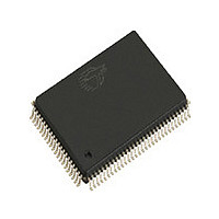
CY7C1380CV25-167AC Cypress Semiconductor Corp, CY7C1380CV25-167AC Datasheet - Page 18

CY7C1380CV25-167AC
Manufacturer Part Number
CY7C1380CV25-167AC
Description
Manufacturer
Cypress Semiconductor Corp
Datasheet
1.CY7C1380CV25-167AC.pdf
(33 pages)
Specifications of CY7C1380CV25-167AC
Density
18Mb
Access Time (max)
3.4ns
Sync/async
Synchronous
Architecture
SDR
Clock Freq (max)
166MHz
Operating Supply Voltage (typ)
2.5V
Address Bus
19b
Package Type
TQFP
Operating Temp Range
0C to 70C
Number Of Ports
4
Supply Current
275mA
Operating Supply Voltage (min)
2.375V
Operating Supply Voltage (max)
2.625V
Operating Temperature Classification
Commercial
Mounting
Surface Mount
Pin Count
100
Word Size
36b
Number Of Words
512K
Lead Free Status / Rohs Status
Not Compliant
Document #: 38-05240 Rev. *C
2.5V TAP AC Test Conditions
Input pulse levels
Input rise and fall time..................................................... 1 ns
Input timing reference levels .........................................1.25V
Output reference levels.................................................1.25V
Test load termination supply voltage.............................1.25V
TAP DC Electrical Characteristics And Operating Conditions
otherwise noted)
Identification Register Definitions
Scan Register Sizes
Identification Codes
V
V
V
V
V
V
I
Revision Number (31:29)
Device Depth (28:24)
Architecture/Memory type(23:18)
Bus Width/Density(17:12)
Cypress JEDEC ID Code (11:1)
ID Register Presence Indicator (0)
Instruction
Bypass
ID
Boundary Scan Order
EXTEST
IDCODE
SAMPLE Z
RESERVED
Note:
11. All voltages referenced to V
X
OH1
OH2
OL1
OL2
IH
IL
Register Name
Parameter
Instruction
Instruction Field
[11]
......................................... V
Output HIGH Voltage
Output HIGH Voltage
Output LOW Voltage
Output LOW Voltage
Input HIGH Voltage
Input LOW Voltage
Input Load Current
Bit Size (x36)
SS
Description
Code
(GND).
000
001
010
011
32
72
3
1
Captures I/O ring contents. Places the boundary scan register between TDI and TDO.
Forces all SRAM outputs to High-Z state. This instruction is not 1149.1 compliant.
Loads the ID register with the vendor ID code and places the register between TDI and
TDO. This operation does not affect SRAM operations.
Captures I/O ring contents. Places the boundary scan register between TDI and TDO.
Forces all SRAM output drivers to a High-Z state.
Do Not Use: This instruction is reserved for future use.
CY7C1380CV25
00000110100
Bit Size (x18)
(512Kx36)
I
I
I
I
GND < V
OH
OH
OL
OL
000000
100101
01011
010
= 8.0 mA
= 100 µA
= -1.0 mA
= -100 µA
1
SS
32
72
Description
3
1
to 2.5V
IN
< V
DDQ
CY7C1382CV25
00000110100
2.5V TAP AC Output Load Equivalent
(1Mx18)
000000
010101
01011
010
1
V
V
V
V
V
V
Conditions
TDO
DDQ
DDQ
DDQ
DDQ
DDQ
DDQ
Description
= 2.5V
= 2.5V
= 2.5V
= 2.5V
= 2.5V
= 2.5V
(0°C < TA < +70°C; Vdd = 2.5V ±0.125V unless
Describes the version number.
Reserved for internal use.
Defines memory type and architecture.
Defines width and density.
Allows unique identification of SRAM vendor.
Indicates the presence of an ID register.
Z = 50
O
Min.
-0.3
2.0
2.1
1.7
-5
Description
CY7C1380CV25
CY7C1382CV25
1.25V
V
DD
Max.
0.4
0.2
0.7
5
+ 0.3
20pF
50
Page 18 of 33
Unit
µA
V
V
V
V
V
V
[+] Feedback


