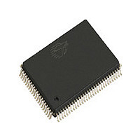
CY7C1370C-167AC Cypress Semiconductor Corp, CY7C1370C-167AC Datasheet - Page 13

CY7C1370C-167AC
Manufacturer Part Number
CY7C1370C-167AC
Description
Manufacturer
Cypress Semiconductor Corp
Datasheet
1.CY7C1370C-167AC.pdf
(27 pages)
Specifications of CY7C1370C-167AC
Density
18Mb
Access Time (max)
3.4ns
Sync/async
Synchronous
Architecture
SDR
Clock Freq (max)
166MHz
Operating Supply Voltage (typ)
3.3V
Address Bus
19b
Package Type
TQFP
Operating Temp Range
0C to 70C
Number Of Ports
1
Supply Current
275mA
Operating Supply Voltage (min)
3.135V
Operating Supply Voltage (max)
3.465V
Operating Temperature Classification
Commercial
Mounting
Surface Mount
Pin Count
100
Word Size
36b
Number Of Words
512K
Lead Free Status / Rohs Status
Not Compliant
Available stocks
Company
Part Number
Manufacturer
Quantity
Price
Company:
Part Number:
CY7C1370C-167AC
Manufacturer:
CYPRESS
Quantity:
230
Part Number:
CY7C1370C-167AC
Manufacturer:
CYPRESS/赛普拉斯
Quantity:
20 000
Document #: 38-05233 Rev. *D
TAP Controller Block Diagram
TAP Electrical Characteristics
TAP AC Switching Characteristics
V
V
V
V
V
V
I
I
t
t
t
t
Notes:
10. All voltage referenced to ground.
11. Overshoot: V
12. t
13. Test conditions are specified using the load in TAP AC test conditions. t
Parameter
X
X
TCYC
TF
TH
TL
Parameter
TDI
OH1
OH2
OL1
OL2
IH
IL
CS
and t
TCK
TMS
CH
refer to the set-up and hold time requirements of latching data from the boundary scan register.
Output HIGH Voltage
Output HIGH Voltage
Output LOW Voltage
Output LOW Voltage
Input HIGH Voltage
Input LOW Voltage
Input Load Current
Input Load Current TMS and TDI
IH
TCK Clock Cycle Time
TCK Clock Frequency
TCK Clock HIGH
TCK Clock LOW
(AC) < V
Selection
Circuitry
DD
+ 1.5V for t < t
Description
TCYC
/2; undershoot: V
Over the Operating Range
31
68
Over the Operating Range
Description
30
Identification Register
.
I
I
I
I
I
I
GND ≤ V
GND ≤ V
OH
OH
OH
OL
OL
OL
Instruction Register
IL
= 8.0 mA
= 1.0 mA
= 100 µA
29
.
= –4.0 mA
= –1.0 mA
= –100 µA
(AC) > −0.5V for t < t
Boundary Scan Register
TAP Controller
I
I
R
.
.
≤ V
≤ V
/t
F
= 1 ns.
Bypass Register
DDQ
DDQ
.
.
Test Conditions
[10, 11]
2
2
2
TCYC
[12, 13]
/2.
V
V
V
V
V
V
V
V
V
V
V
V
1
1
1
DDQ
DDQ
DDQ
DDQ
DDQ
DDQ
DDQ
DDQ
DDQ
DDQ
DDQ
DDQ
0
0
0
0
= 3.3V
= 2.5V
= 3.3V
= 2.5V
= 3.3V
= 2.5V
= 3.3V
= 2.5V
= 3.3V
= 2.5V
= 3.3V
= 2.5V
Min.
100
Selection
Circuitry
40
40
Min.
–0.5
–0.3
2.4
1.7
2.9
2.1
2.0
1.7
–5
–5
CY7C1370C
CY7C1372C
Max.
10
V
V
DD
DD
Max.
Page 13 of 27
0.4
0.4
0.2
0.2
0.7
0.7
5
5
+ 0.3
+ 0.3
TDO
MHz
Unit
ns
ns
ns
Unit
µA
µA
V
V
V
V
V
V
V
V
V
V
[+] Feedback


