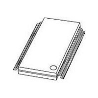
PCF8562TT NXP Semiconductors, PCF8562TT Datasheet - Page 22

PCF8562TT
Manufacturer Part Number
PCF8562TT
Description
Manufacturer
NXP Semiconductors
Datasheet
1.PCF8562TT.pdf
(36 pages)
Specifications of PCF8562TT
Operating Supply Voltage (typ)
2.5/3.3/5V
Number Of Digits
16
Number Of Segments
128
Operating Temperature (min)
-40C
Operating Temperature (max)
85C
Operating Temperature Classification
Industrial
Package Type
TSSOP
Pin Count
48
Mounting
Surface Mount
Power Dissipation
400mW
Frequency (max)
400KHz
Operating Supply Voltage (min)
1.8V
Operating Supply Voltage (max)
5.5V
Lead Free Status / Rohs Status
Compliant
Available stocks
Company
Part Number
Manufacturer
Quantity
Price
Part Number:
PCF8562TT
Manufacturer:
NXP/恩智浦
Quantity:
20 000
Company:
Part Number:
PCF8562TT/2
Manufacturer:
NXP Semiconductors
Quantity:
36 137
Company:
Part Number:
PCF8562TT/2
Manufacturer:
NXP
Quantity:
12 000
Part Number:
PCF8562TT/2
Manufacturer:
NXP/恩智浦
Quantity:
20 000
Company:
Part Number:
PCF8562TT/2Ј¬118
Manufacturer:
NXP
Quantity:
64 000
NXP Semiconductors
Table 6.
[1]
PCF8562_2
Product data sheet
Command
Mode Set
Load Data
Pointer
Device
Select
Bank Select C
Blink
Not used.
Definition of PCF8562 commands
Operation code
C
C
C
C
7.8 Command decoder
1
0
1
1
1
The command decoder identifies command bytes that arrive on the I
commands carry a continuation bit C in their most significant bit position as shown in
Figure
also represent a command. If this bit is reset, it indicates that the command byte is the last
in the transfer. Further bytes will be regarded as display data.
The five commands available to the PCF8562 are defined in
Table 7.
LCD drive mode
Drive mode
static
1 : 2
1 : 3
1 : 4
0
1
1
P5
1
16. When this bit is set, it indicates that the next byte of the transfer to arrive will
[1]
P4
0
1
1
Mode set option 1
E
P3
0
1
0
Rev. 02 — 22 January 2007
B
P2
A2
0
A
Backplane
BP0
BP0, BP1
BP0, BP1, BP2
BP0, BP1, BP2, BP3
M1
P1
A1
I
BF1
M0
P0
A0
O
BF0
Options
Table 7
Table 8
Table 9
Table 10
Table 11
Table 12
Table 13
Table 14
Table 15
Universal LCD driver for low multiplex rates
Description
Defines LCD Drive mode.
Defines LCD bias configuration.
Defines display status; the possibility
to disable the display allows
implementation of blinking under
external control.
6 bits of immediate data, bits
P5 to P0 are transferred to the data
pointer to define one of 32 display
RAM addresses.
3 bits of immediate data, bits
A0 to A2 are transferred to the
subaddress counter to define one of
8 hardware subaddresses.
Defines the input bank selection
(storage of arriving display data).
Defines the output bank selection
(retrieval of LCD display data); the
BANK SELECT command has no
effect in 1 : 3 and 1 : 4 multiplex drive
modes.
Defines the blink frequency
Selects the blink mode; normal
operation with frequency set by BF1,
BF0 or blinking by alternate display
RAM banks; alternate RAM blinking
does not apply in 1 : 3 and 1 : 4
multiplex drive modes.
0
1
1
0
Table
M1
6.
2
C-bus. All available
PCF8562
© NXP B.V. 2007. All rights reserved.
Bit
1
0
1
0
M0
22 of 36


