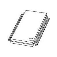
PCF8562TT NXP Semiconductors, PCF8562TT Datasheet - Page 15

PCF8562TT
Manufacturer Part Number
PCF8562TT
Description
Manufacturer
NXP Semiconductors
Datasheet
1.PCF8562TT.pdf
(36 pages)
Specifications of PCF8562TT
Operating Supply Voltage (typ)
2.5/3.3/5V
Number Of Digits
16
Number Of Segments
128
Operating Temperature (min)
-40C
Operating Temperature (max)
85C
Operating Temperature Classification
Industrial
Package Type
TSSOP
Pin Count
48
Mounting
Surface Mount
Power Dissipation
400mW
Frequency (max)
400KHz
Operating Supply Voltage (min)
1.8V
Operating Supply Voltage (max)
5.5V
Lead Free Status / Rohs Status
Compliant
Available stocks
Company
Part Number
Manufacturer
Quantity
Price
Part Number:
PCF8562TT
Manufacturer:
NXP/恩智浦
Quantity:
20 000
Company:
Part Number:
PCF8562TT/2
Manufacturer:
NXP Semiconductors
Quantity:
36 137
Company:
Part Number:
PCF8562TT/2
Manufacturer:
NXP
Quantity:
12 000
Part Number:
PCF8562TT/2
Manufacturer:
NXP/恩智浦
Quantity:
20 000
Company:
Part Number:
PCF8562TT/2Ј¬118
Manufacturer:
NXP
Quantity:
64 000
NXP Semiconductors
PCF8562_2
Product data sheet
6.10 Display RAM
The display RAM is a static 32
bit-map indicates the on-state of the corresponding LCD segment; similarly, a logic 0
indicates the off-state. There is a one-to-one correspondence between the RAM
addresses and the segment outputs, and between the individual bits of a RAM word and
the backplane outputs. The first RAM column corresponds to the 32 segments operated
with respect to backplane BP0 (see
segment data of the second, third and fourth column of the display RAM are
time-multiplexed with BP1, BP2 and BP3 respectively.
When display data is transmitted to the PCF8562, the display bytes received are stored in
the display RAM in accordance with the selected LCD drive mode. The data is stored as it
arrives and does not wait for an acknowledge cycle as with the commands. Depending on
the current multiplex drive mode, data is stored singularly, in pairs, triplets or quadruplets.
For example, in the 1 : 2 mode, the RAM data is stored every second bit. To illustrate the
filling order, an example of a 7-segment numeric display showing all drive modes is given
in
With reference to
placed in bit 0 of eight successive display RAM addresses. In the 1 : 2 mode, the eight
transmitted data bits are placed in bits 0 and 1 of four successive display RAM addresses.
In the 1 : 3 mode, these bits are placed in bits 0, 1 and 2 of three successive addresses,
with bit 2 of the third address left unchanged. This last bit may, if necessary, be controlled
by an additional transfer to this address but care should be taken to avoid overriding
adjacent data because full bytes are always transmitted.
In the 1 : 4 mode, the eight transmitted data bits are placed in bits 0, 1, 2 and 3 of two
successive display RAM addresses.
Fig 9. Display RAM bit-map showing direct relationship between display RAM addresses
Figure
backplane outputs
display RAM bits
and segment outputs also between bits in a RAM word and the backplane outputs
9; the RAM filling organization depicted applies equally to other LCD types.
(columns) /
(BP)
Figure
0
1
2
3
Rev. 02 — 22 January 2007
0
9, in the static drive mode, the eight transmitted data bits are
1
2
4-bit RAM which stores LCD data. A logic 1 in the RAM
display RAM addresses (rows) / segment outputs (S)
3
Figure
4
Universal LCD driver for low multiplex rates
9). In multiplexed LCD applications the
27
28
PCF8562
© NXP B.V. 2007. All rights reserved.
29
001aac265
30
31
15 of 36


