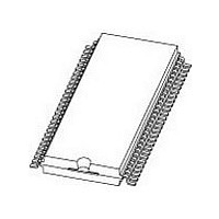
PCF8576CT NXP Semiconductors, PCF8576CT Datasheet - Page 26

PCF8576CT
Manufacturer Part Number
PCF8576CT
Description
Manufacturer
NXP Semiconductors
Datasheet
1.PCF8576CT.pdf
(56 pages)
Specifications of PCF8576CT
Operating Supply Voltage (typ)
2.5/3.3/5V
Number Of Digits
20
Number Of Segments
160
Package Type
VSO
Pin Count
56
Mounting
Surface Mount
Power Dissipation
400mW
Frequency (max)
315KHz
Operating Supply Voltage (min)
2V
Operating Supply Voltage (max)
6V
Lead Free Status / Rohs Status
Compliant
Available stocks
Company
Part Number
Manufacturer
Quantity
Price
Part Number:
PCF8576CT
Manufacturer:
PHILIPS/飞利浦
Quantity:
20 000
Part Number:
PCF8576CT/1
Manufacturer:
NXP/恩智浦
Quantity:
20 000
Part Number:
PCF8576CT/1,518
Manufacturer:
NXP/恩智浦
Quantity:
20 000
Company:
Part Number:
PCF8576CT/1112
Manufacturer:
NXP Semiconductors
Quantity:
135
Company:
Part Number:
PCF8576CT/1118
Manufacturer:
NXPSemicondu
Quantity:
2 802
Company:
Part Number:
PCF8576CT/1Ј¬112
Manufacturer:
NXP
Quantity:
880
Company:
Part Number:
PCF8576CT/1Ј¬118
Manufacturer:
NXP
Quantity:
21 000
Part Number:
PCF8576CT/F1
Manufacturer:
PHILIPS/飞利浦
Quantity:
20 000
Part Number:
PCF8576CTT
Manufacturer:
NXP/恩智浦
Quantity:
20 000
NXP Semiconductors
Table 8.
PCF8576C_9
Product data sheet
Command
mode set
load data
pointer
device select C
bank select
blink
Definition of PCF8576C commands
OPCODE
Bit 7 Bit 6 Bit 5 Bit 4 Bit 3 Bit 2 Bit 1 Bit 0
C
C
C
C
8.3 Command decoder
1
0
1
1
1
The command decoder identifies command bytes that arrive on the I
commands carry a continuation bit C in their most significant bit position as shown in
Figure
also represent a command. If this bit is reset, it indicates that the command byte is the last
in the transfer. Further bytes will be regarded as display data.
The five commands available to the PCF8576C are defined in
Fig 18. I
Fig 19. General format of byte command
0
P5
1
1
1
(1) C = 0; last command
(2) C = 1; commands continue
19. When this bit is set, it indicates that the next byte of the transfer to arrive will
LP
P4
0
1
1
2
S
C-bus protocol
0 1 1 1 0 0
E
P3
0
1
0
slave address
1 byte
B
P2
A2
0
A
Rev. 09 — 9 July 2009
S
A
0
M1
P1
A1
I
BF1
R/W
MSB
0 A C
C
M0
P0
A0
O
BF0
acknowledge by
all addressed
n
PCF8576Cs
Reference
Section 8.3.1
Section 8.3.2
Section 8.3.3
Section 8.3.4
Section 8.3.5
COMMAND
REST OF OPCODE
1 byte(s)
Universal LCD driver for low multiplex rates
A
Description
defines LCD drive mode, LCD bias
configuration, display status and power
dissipation mode
data pointer to define one of 40 display
RAM addresses
define one of eight hardware
subaddresses
bit I: defines input bank selection
(storage of arriving display data);
bit O: defines output bank selection
(retrieval of LCD display data)
defines the blink frequency and blink
mode
msa833
DISPLAY DATA
n
LSB
0 byte(s)
Table
by A0, A1 and A2
update data pointers
subaddress counter
PCF8576C only
PCF8576C
and if necessary,
acknowledge
8.
2
C-bus. All available
selected
© NXP B.V. 2009. All rights reserved.
A
P
mbe538
26 of 56


