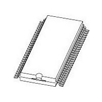
PCF8576CT NXP Semiconductors, PCF8576CT Datasheet - Page 22

PCF8576CT
Manufacturer Part Number
PCF8576CT
Description
Manufacturer
NXP Semiconductors
Datasheet
1.PCF8576CT.pdf
(56 pages)
Specifications of PCF8576CT
Operating Supply Voltage (typ)
2.5/3.3/5V
Number Of Digits
20
Number Of Segments
160
Package Type
VSO
Pin Count
56
Mounting
Surface Mount
Power Dissipation
400mW
Frequency (max)
315KHz
Operating Supply Voltage (min)
2V
Operating Supply Voltage (max)
6V
Lead Free Status / Rohs Status
Compliant
Available stocks
Company
Part Number
Manufacturer
Quantity
Price
Part Number:
PCF8576CT
Manufacturer:
PHILIPS/飞利浦
Quantity:
20 000
Part Number:
PCF8576CT/1
Manufacturer:
NXP/恩智浦
Quantity:
20 000
Part Number:
PCF8576CT/1,518
Manufacturer:
NXP/恩智浦
Quantity:
20 000
Company:
Part Number:
PCF8576CT/1112
Manufacturer:
NXP Semiconductors
Quantity:
135
Company:
Part Number:
PCF8576CT/1118
Manufacturer:
NXPSemicondu
Quantity:
2 802
Company:
Part Number:
PCF8576CT/1Ј¬112
Manufacturer:
NXP
Quantity:
880
Company:
Part Number:
PCF8576CT/1Ј¬118
Manufacturer:
NXP
Quantity:
21 000
Part Number:
PCF8576CT/F1
Manufacturer:
PHILIPS/飞利浦
Quantity:
20 000
Part Number:
PCF8576CTT
Manufacturer:
NXP/恩智浦
Quantity:
20 000
NXP Semiconductors
PCF8576C_9
Product data sheet
7.14.2 Input bank selector
7.15 Blinker
The PCF8576C includes a RAM bank switching feature in the static and 1:2 multiplex
drive modes. In the static drive mode, the bank select command may request the contents
of bit 2 to be selected for display instead of the contents of bit 0. In 1:2 multiplex drive
mode, the contents of bits 2 and 3 may be selected instead of bits 0 and 1. This enables
preparation of display information in an alternative bank and the ability to switch to it once
it has been assembled.
The input bank selector (see
the selected LCD drive configuration. Using the bank select command, display data can
be loaded in bit 2 into static drive mode or in bits 2 and 3 into 1:2 multiplex drive mode.
The input bank selector functions independently of the output bank selector.
The display blinking capabilities of the PCF8576C are very versatile. The whole display
can be blinked at frequencies selected by the blink command. The blinking frequencies
are integer fractions of the clock frequency; the ratios between the clock and blinking
frequencies depend on the mode in which the device is operating (see
Table 7.
An additional feature is for an arbitrary selection of LCD segments to be blinked. This
applies to the static and 1:2 multiplex drive modes and can be implemented without any
communication overheads. Using the output bank selector, the displayed RAM banks are
exchanged with alternate RAM banks at the blinking frequency. This mode can also be
specified by the blink command (see
In the 1:3 and 1:4 multiplex modes, where no alternate RAM bank is available, groups of
LCD segments can be blinked by selectively changing the display RAM data at fixed time
intervals.
If the entire display needs to be blinked at a frequency other than the nominal blink
frequency, this can be done using the mode set command to set and reset the display
enable bit E at the required rate (see
Blinking mode
off
1
2
3
Blink frequencies
Normal operating
mode ratio
-
f
f
f
blink
blink
blink
Rev. 09 — 9 July 2009
=
=
=
Table
--------------- -
92160
------------------- -
184320
------------------- -
368640
f
f
f
clk
clk
clk
15) loads display data into the display RAM based on
Table
Table
Universal LCD driver for low multiplex rates
16).
9).
Power saving mode
ratio
-
f
f
f
blink
blink
blink
=
=
=
--------------- -
15360
--------------- -
30720
--------------- -
61440
f
f
f
clk
clk
clk
PCF8576C
Blink frequency
blinking off
2 Hz
1 Hz
0.5 Hz
Table
© NXP B.V. 2009. All rights reserved.
7).
22 of 56


