IDT74LVCH245AQ IDT, Integrated Device Technology Inc, IDT74LVCH245AQ Datasheet - Page 2
IDT74LVCH245AQ
Manufacturer Part Number
IDT74LVCH245AQ
Description
Manufacturer
IDT, Integrated Device Technology Inc
Datasheet
1.IDT74LVCH245AQ.pdf
(6 pages)
Specifications of IDT74LVCH245AQ
Logic Family
LVC
Operating Supply Voltage (typ)
3.3V
Propagation Delay Time
9.5ns
Number Of Elements
1
Number Of Channels
8
Input Logic Level
LVTTL
Output Logic Level
LVTTL
Output Type
3-State
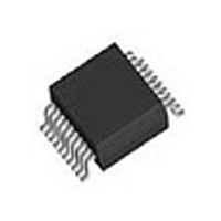
Package Type
SSOP
Polarity
Non-Inverting
Logical Function
Bus Transceiver
Operating Supply Voltage (min)
2.7V
Operating Supply Voltage (max)
3.6V
Technology
CMOS
Operating Temp Range
-40C to 85C
Operating Temperature Classification
Industrial
Mounting
Surface Mount
Pin Count
20
Lead Free Status / Rohs Status
Not Compliant
Available stocks
Company
Part Number
Manufacturer
Quantity
Price
Company:

Part Number:
IDT74LVCH245AQ
Manufacturer:
IDT
Quantity:
6 220


PIN CONFIGURATION
IDT74LVCH245A
3.3V CMOS OCTAL BUS TRANSCEIVER WITH 3-STATE OUTPUTS
GND
DIR
A
A
A
A
A
A
A
A
4
3
5
2
6
7
8
1
SSOP/ QSOP/ TSSOP
1
4
2
5
8
3
6
7
9
10
TOP VIEW
19
15
17
20
18
16
14
13
12
11
V
OE
B
B
B
B
B
B
B
B
CC
1
3
4
5
6
7
8
2
2
CAPACITANCE
NOTE:
1. As applicable to the device type.
PIN DESCRIPTION
NOTE:
1. These pins have "Bus-Hold". All other pins are standard inputs, outputs, or I/Os.
FUNCTION TABLE
ABSOLUTE MAXIMUM RATINGS
NOTE:
1. Stresses greater than those listed under ABSOLUTE MAXIMUM RATINGS may cause
NOTES:
1. H = HIGH Voltage Level
Symbol
V
T
I
I
I
I
I
C
Symbol
C
C
CC
OUT
IK
OK
SS
Pin Names
STG
TERM
permanent damage to the device. This is a stress rating only and functional operation
of the device at these or any other conditions above those indicated in the operational
sections of this specification is not implied. Exposure to absolute maximum rating
conditions for extended periods may affect reliability.
IN
X = Don’t Care
L = LOW Voltage Level
Z = High-Impedance
OUT
I/O
OE
H
L
L
DIR
OE
A x
B x
Inputs
Terminal Voltage with Respect to GND
Storage Temperature
DC Output Current
Continuous Clamp Current,
V
Continuous Current through each
V
Input Capacitance
Output Capacitance
I/O Port Capacitance
I
CC
< 0 or V
Parameter
or GND
DIR
H
X
L
O
Output Enable Input (Active LOW)
Direction Control Input
Data Inputs
Data Outputs
Description
< 0
(1)
(T
(1)
Bus B Data to Bus A
Bus A Data to Bus B
Z
A
INDUSTRIAL TEMPERATURE RANGE
= +25°C, F = 1.0MHz)
(1)
Conditions
V
V
V
OUT
Description
IN
IN
= 0V
= 0V
= 0V
Outputs
Typ.
4.5
5.5
6.5
–0.5 to +6.5
–65 to +150
–50 to +50
±100
Max
–50
Max.
6
8
8
(1)
Unit
Unit
pF
pF
pF
mA
mA
mA
° C
V
Related parts for IDT74LVCH245AQ
Image
Part Number
Description
Manufacturer
Datasheet
Request
R

Part Number:
Description:
TRANSLATION DEVICE DPI 80-PQFP
Manufacturer:
IDT, Integrated Device Technology Inc
Datasheet:
Part Number:
Description:
IDT PART
Manufacturer:
IDT, Integrated Device Technology Inc
Datasheet:
Part Number:
Description:
IC LIU T1/E1/J1 OCTAL 256PBGA
Manufacturer:
IDT, Integrated Device Technology Inc
Datasheet:

Part Number:
Description:
IC FREQ TIMING GENERATOR 28TSSOP
Manufacturer:
IDT, Integrated Device Technology Inc
Datasheet:
Part Number:
Description:
IC CLK DVR PLL 1:10 40VFQFPN
Manufacturer:
IDT, Integrated Device Technology Inc
Datasheet:
Part Number:
Description:
IC CLK FANOUT BUFFER 1:18 32LQFP
Manufacturer:
IDT, Integrated Device Technology Inc
Datasheet:
Part Number:
Description:
IC CLK FANOUT BUFFER 1:18 32LQFP
Manufacturer:
IDT, Integrated Device Technology Inc
Datasheet:
Part Number:
Description:
IC CK505 VREG/RES 56TSSOP
Manufacturer:
IDT, Integrated Device Technology Inc
Datasheet:

Part Number:
Description:
IC SDRAM CLK DVR 1:10 48-TSSOP
Manufacturer:
IDT, Integrated Device Technology Inc
Datasheet:

Part Number:
Description:
IC CLK DVR PLL 1:10 48TSSOP
Manufacturer:
IDT, Integrated Device Technology Inc
Datasheet:
Part Number:
Description:
IC FLEXPC CLK PROGR P4 56-TSSOP
Manufacturer:
IDT, Integrated Device Technology Inc
Datasheet:
Part Number:
Description:
IC FLEXPC CLK PROGR P4 56-TSSOP
Manufacturer:
IDT, Integrated Device Technology Inc
Datasheet:
Part Number:
Description:
IC FLEXPC CLK PROGR P4 56-SSOP
Manufacturer:
IDT, Integrated Device Technology Inc
Datasheet:

Part Number:
Description:
IC PLL CLK DRIVER 2.5V 28-TSSOP
Manufacturer:
IDT, Integrated Device Technology Inc
Datasheet:
Part Number:
Description:
IC CLOCK DRIVER 2.5V 24-TSSOP
Manufacturer:
IDT, Integrated Device Technology Inc
Datasheet: