INA-31063 Avago Technologies US Inc., INA-31063 Datasheet - Page 6
INA-31063
Manufacturer Part Number
INA-31063
Description
Manufacturer
Avago Technologies US Inc.
Datasheet
1.INA-31063.pdf
(11 pages)
Specifications of INA-31063
Manufacturer's Type
RFIC Amplifier
Number Of Channels
1
Supply Current
13.5@3VmA
Frequency (max)
2.5GHz
Operating Supply Voltage (typ)
3V
Operating Supply Voltage (max)
6V
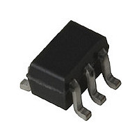
Package Type
SOT-363
Mounting
Surface Mount
Pin Count
6
Noise Figure (typ)
6.1@1900MHzdB
Lead Free Status / Rohs Status
Not Compliant
Available stocks
Company
Part Number
Manufacturer
Quantity
Price
Company:

Part Number:
INA-31063-TR1
Manufacturer:
INA
Quantity:
8 123


Figure 14 shows an assembled
50
is fed directly into the V
the INA-31063 and into the RF
Output pin through the RF choke
(RFC). Capacitor C3 provides RF
bypassing for both the V
the power supply end of the RFC.
Capacitor C4 is optional and may
be used to add additional
bypassing for the V
bypassed V
necessary in cascades of ampli-
fier stages to prevent oscillation
that may occur as a result of RF
feedback through the power
supply lines.
900 MHz 50
Example
The use of a simple impedance
matching network will typically
increase both gain and output
power by 1.5 dB and 1.5 dBm,
respectively. The values that were
chosen for the two tuning ele-
ments were a 12 nF series induc-
tor and a 1.0 pF shunt capacitor.
The RF choke was a 56 nH
(Coilcraft 1008CS-221, TOKO
LL2012-F or equivalent). The two
Figure 14. Assembled Amplifier.
amplifier. The +3 volt supply
d
line is especially
Matched
INA-3XX63 DEMO BOARD
d
line. A well-
d
d
C1
C3
pin of
pin and
31
Ctune
RFC
Ltune
blocking capacitors were 100 pF
and the bypass capacitor was
1000 pF.
Figure 15. Impedance Matched
Output Amplifier Circuit.
These values provide excellent
amplifier performance at 900 MHz.
Larger values for the choke and
capacitors can be used to extend
the lower end of the bandwidth. A
convenient method for making RF
connection to the demonstration
board is to use a PCB mounting
type of SMA connector (Johnson
142-0701881, or equivalent). These
connectors can be slipped over
the edge of the PCB and the
center conductor soldered to the
input and output lines. The ground
pins of the connectors can be
soldered to the ground plane on
the backside of board.
Input
RF
C
C2
shunt
C
V
block
d
C4
RFM
RFC
C
bypass
C
out
Output
RF
V
d
Figure 16. Suggested Matching
Elements for Common Frequency
Bands.
The test results for the INA-31063
were measured on the 50
and output impedance matched
amplifier described above.
Figure 17. Measured Input Power vs.
Output Power on Assembled 50
Amplifier at 900 MHz and 1900 MHz.
An important specification when
selecting a LO buffer amplifier is
reverse isolation under P
conditions. Figure 18 shows the
measured reverse isolation with
-10 dBm applied to the input of
the device.
Figure 18. Measured Isolation.
Frequency
1900 MHz
2400 MHz
400 M Hz 120 nH 27 nH
900 MHz
-12
-16
-20
-30
-40
-50
-60
-8
-4
4
0
-30
6
0
-25
0.5
900 MHz
1900 MHz
56 nH 12 nH
33 nH
27 nH
FREQUENCY (GHz)
RFC
-20
1.0
P
in
-15
(dBm)
4.7 nH None
1.8 nH None
RFM
1.5
-10
1 dB
2.0
-5
C
2.7 pF
1.0 pF
input
SHUNT
input
2.5
0
Related parts for INA-31063
Image
Part Number
Description
Manufacturer
Datasheet
Request
R

Part Number:
Description:
OPTOCOUPLER GATE DRV 2A 16-SOIC
Manufacturer:
Avago Technologies US Inc.
Datasheet:
Part Number:
Description:
OPTOCOUPLER 2CH 2.5A 16-SOIC
Manufacturer:
Avago Technologies US Inc.
Datasheet:

Part Number:
Description:
OPTOCOUPLER GATE DRV 0.4A 16SOIC
Manufacturer:
Avago Technologies US Inc.
Datasheet:

Part Number:
Description:
OPTOCOUPLER 2.0A 250KHZ 8-DIP
Manufacturer:
Avago Technologies US Inc.
Datasheet:

Part Number:
Description:
OPTOCOUPLER 2.0A 250KHZ GW 8-SMD
Manufacturer:
Avago Technologies US Inc.
Datasheet:

Part Number:
Description:
OPTOCOUPLER 2CH 15MBD 3.3V 8SOIC
Manufacturer:
Avago Technologies US Inc.
Datasheet:
Part Number:
Description:
OPTOCOUPLER DARL-OUT 8-DIP
Manufacturer:
Avago Technologies US Inc.
Datasheet:
Part Number:
Description:
OPTOCOUPLER IGBT DRIVE 0.4A 8DIP
Manufacturer:
Avago Technologies US Inc.
Datasheet:
Part Number:
Description:
OPTOCOUPLER DARL-OUT 8-DIP
Manufacturer:
Avago Technologies US Inc.
Datasheet:

Part Number:
Description:
OPTOCOUPLER 1CH 1MBS 8-SMD GW
Manufacturer:
Avago Technologies US Inc.
Datasheet:
Part Number:
Description:
OPTOCOUPLER GATE DRIVER 8-DIP
Manufacturer:
Avago Technologies US Inc.
Datasheet:

Part Number:
Description:
OPTOCOUPLER GATE DRIVER 8-SMD
Manufacturer:
Avago Technologies US Inc.
Datasheet:

Part Number:
Description:
OPTOCOUPLER PHOTOTRANS 4-SMD
Manufacturer:
Avago Technologies US Inc.
Datasheet:

Part Number:
Description:
OPTOCOUPLER W/BASE 6-DIP
Manufacturer:
Avago Technologies US Inc.
Datasheet:

Part Number:
Description:
ISOLAT 5KVRMS 4CH TRANS 16SMD GW
Manufacturer:
Avago Technologies US Inc.
Datasheet: