INA-31063 Avago Technologies US Inc., INA-31063 Datasheet - Page 5
INA-31063
Manufacturer Part Number
INA-31063
Description
Manufacturer
Avago Technologies US Inc.
Datasheet
1.INA-31063.pdf
(11 pages)
Specifications of INA-31063
Manufacturer's Type
RFIC Amplifier
Number Of Channels
1
Supply Current
13.5@3VmA
Frequency (max)
2.5GHz
Operating Supply Voltage (typ)
3V
Operating Supply Voltage (max)
6V
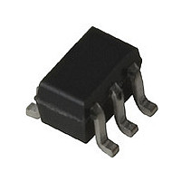
Package Type
SOT-363
Mounting
Surface Mount
Pin Count
6
Noise Figure (typ)
6.1@1900MHzdB
Lead Free Status / Rohs Status
Not Compliant
Available stocks
Company
Part Number
Manufacturer
Quantity
Price
Company:

Part Number:
INA-31063-TR1
Manufacturer:
INA
Quantity:
8 123


INA-31063 Applications
Information
Introduction
The INA-31063 is a +3 volt silicon
RFIC amplifier that is designed
with a two stage internal network
to provide a broadband gain and
50
impedance. With a P
pressed output power of -3 dBm
and high isolation of 40 dB, the
INA-31063 is well suited for LO
buffer amplifier applications in
mobile communication systems.
The 200
the amplifier allows easy connec-
tions to additional RFICs and
some filters.
In addition to use in buffer
applications in the cellular
market, the INA-31063 will find
many applications in battery
operated wireless communication
systems.
Operating Details
The INA-31063 is a voltage biased
device that operates from a
+3 volt power supply with a
typical current drain of 11 mA.
All bias regulation circuitry is
integrated into the RFIC.
Figure 10 shows a typical imple-
mentation of the INA-31063. The
supply voltage for the INA-31063
must be applied to two terminals,
the V
Figure 10. Basic Amplifier
Application.
Input
RF
C
block
d
input and 200
Gnd2
Gnd1
pin and the RF Output pin.
output impedance of
-l dB
Gnd1
output
com-
RFC
C
C
out
bypass
Output
RF
V
d
The V
fier is RF bypassed by placing a
capacitor to ground near the V
pin of the amplifier package. The
power supply connection to the
RF Output pin is achieved by
means of a RF choke (inductor).
The value of the RF choke must
be large relative to 50
to prevent loading of the RF
Output. The supply voltage end of
the RF choke is bypassed to
ground with a capacitor. If the
physical layout permits, this can
be the same bypass capacitor that
is used at the V
amplifier. Blocking capacitors are
normally placed in series with the
RF Input and the RF Output to
isolate the DC voltages on these
pins from circuits adjacent to the
amplifier. The values for the
blocking and bypass capacitors
are selected to provide a reac-
tance at the lowest frequency of
operation that is small relative to
50 . Since the gain of the
INA-31063 extends down to DC,
the frequency response of the
amplifier is limited only by the
values of the capacitors and
choke.
RF Layout
An example for the RF layout for
the INA-31063 is shown in
Figure 11.
Figure 11. RF Layout
This example uses a
microstripline design (solid
groundplane on the backside of
d
50
connection to the ampli-
Gnd 1
Gnd 1
d
terminal of the
50
RF Output
and V d
Gnd 2
in order
d
the circuit board). The circuit
board material is 0.031-inch thick
FR4. Plated through holes (vias)
are used to bring the ground to
the top side of the circuit where
needed. The performance of
INA-31063 is sensitive to ground
path inductance. The two-stage
design creates the possibility of a
feedback loop being formed
through the ground returns of the
stages, Gnd 1 and Gnd 2.
Figure 12. INA-31063 Potential
Ground Loop.
Figure 13. INA-31063 Suggested
Layout.
At least one ground via should be
placed adjacent to each ground
pin to assure good RF grounding.
Multiple vias are used to reduce
the inductance of the path to
ground and should be placed as
close to the package terminals as
practical.
The effects of the potential
ground loop shown in Figure 12
may be observed as a “peaking” in
the gain versus frequency
response, an increase in input
VSWR, or even as return gain at
the input of the INA-31063.
5
VIA
Gnd 1
Gnd 1
VIA
Gnd 2
Gnd 2
VIA
Related parts for INA-31063
Image
Part Number
Description
Manufacturer
Datasheet
Request
R

Part Number:
Description:
OPTOCOUPLER GATE DRV 2A 16-SOIC
Manufacturer:
Avago Technologies US Inc.
Datasheet:
Part Number:
Description:
OPTOCOUPLER 2CH 2.5A 16-SOIC
Manufacturer:
Avago Technologies US Inc.
Datasheet:

Part Number:
Description:
OPTOCOUPLER GATE DRV 0.4A 16SOIC
Manufacturer:
Avago Technologies US Inc.
Datasheet:

Part Number:
Description:
OPTOCOUPLER 2.0A 250KHZ 8-DIP
Manufacturer:
Avago Technologies US Inc.
Datasheet:

Part Number:
Description:
OPTOCOUPLER 2.0A 250KHZ GW 8-SMD
Manufacturer:
Avago Technologies US Inc.
Datasheet:

Part Number:
Description:
OPTOCOUPLER 2CH 15MBD 3.3V 8SOIC
Manufacturer:
Avago Technologies US Inc.
Datasheet:
Part Number:
Description:
OPTOCOUPLER DARL-OUT 8-DIP
Manufacturer:
Avago Technologies US Inc.
Datasheet:
Part Number:
Description:
OPTOCOUPLER IGBT DRIVE 0.4A 8DIP
Manufacturer:
Avago Technologies US Inc.
Datasheet:
Part Number:
Description:
OPTOCOUPLER DARL-OUT 8-DIP
Manufacturer:
Avago Technologies US Inc.
Datasheet:

Part Number:
Description:
OPTOCOUPLER 1CH 1MBS 8-SMD GW
Manufacturer:
Avago Technologies US Inc.
Datasheet:
Part Number:
Description:
OPTOCOUPLER GATE DRIVER 8-DIP
Manufacturer:
Avago Technologies US Inc.
Datasheet:

Part Number:
Description:
OPTOCOUPLER GATE DRIVER 8-SMD
Manufacturer:
Avago Technologies US Inc.
Datasheet:

Part Number:
Description:
OPTOCOUPLER PHOTOTRANS 4-SMD
Manufacturer:
Avago Technologies US Inc.
Datasheet:

Part Number:
Description:
OPTOCOUPLER W/BASE 6-DIP
Manufacturer:
Avago Technologies US Inc.
Datasheet:

Part Number:
Description:
ISOLAT 5KVRMS 4CH TRANS 16SMD GW
Manufacturer:
Avago Technologies US Inc.
Datasheet: