OM13001,598 NXP Semiconductors, OM13001,598 Datasheet - Page 90
OM13001,598
Manufacturer Part Number
OM13001,598
Description
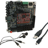
EA LPC177X/8X EVAL BOARD
Manufacturer
NXP Semiconductors
Series
-r
Type
MCUr
Specifications of OM13001,598
Contents
Board, Cable, Headphones, Registration Card
Lead Free Status / Rohs Status
Lead free / RoHS Compliant
For Use With/related Products
LPC1788
Other names
568-6707


NXP Semiconductors
LPC178X_7X
Objective data sheet
Fig 24. I
SDA
SCL
2
C-bus pins clock timing
70 %
30 %
S
t
f
t
f
70 %
Table 23.
T
[1]
[2]
[3]
[4]
[5]
[6]
[7]
[8]
[9]
[10] A Fast-mode I
30 %
Symbol
t
t
HD;DAT
SU;DAT
amb
See the I
Parameters are valid over operating temperature range unless otherwise specified.
t
and the acknowledge.
A device must internally provide a hold time of at least 300 ns for the SDA signal (with respect to the
V
C
The maximum t
output stage t
SDA and the SCL pins and the SDA/SCL bus lines without exceeding the maximum specified t
In Fast-mode Plus, fall time is specified the same for both output stage and bus timing. If series resistors
are used, designers should allow for this when considering bus timing.
The maximum t
the maximum of t
the device does not stretch the LOW period (t
data must be valid by the set-up time before it releases the clock.
t
transmission and the acknowledge.
250 ns must then be met. This will automatically be the case if the device does not stretch the LOW period
of the SCL signal. If such a device does stretch the LOW period of the SCL signal, it must output the next
data bit to the SDA line t
specification) before the SCL line is released. Also the acknowledge timing must meet this set-up time.
1 / f
HD;DAT
SU;DAT
=
IH
b
= total capacitance of one bus line in pF.
(min) of the SCL signal) to bridge the undefined region of the falling edge of SCL.
SCL
40
is the data hold time that is measured from the falling edge of SCL; applies to data in transmission
is the data set-up time that is measured with respect to the rising edge of SCL; applies to data in
Dynamic characteristic: I
t
C to +85
2
HD;DAT
C-bus specification UM10204 for details.
Parameter
data hold time
data set-up
time
70 %
30 %
70 %
f
2
30 %
All information provided in this document is subject to legal disclaimers.
is specified at 250 ns. This allows series protection resistors to be connected in between the
C-bus device can be used in a Standard-mode I
HD;DAT
f
for the SDA and SCL bus lines is specified at 300 ns. The maximum fall time for the SDA
VD;DAT
t
SU;DAT
C.
could be 3.45 s and 0.9 s for Standard-mode and Fast-mode but must be less than
[2]
or t
r(max)
Rev. 2 — 27 May 2011
VD;ACK
[3][4][8]
[9][10]
+ t
70 %
SU;DAT
30 %
by a transition time (see UM10204). This maximum must only be met if
t
2
LOW
= 1000 + 250 = 1250 ns (according to the Standard-mode I
C-bus pins
Conditions
Standard-mode
Fast-mode
Fast-mode Plus
Standard-mode
Fast-mode
Fast-mode Plus
LOW
) of the SCL signal. If the clock stretches the SCL, the
t
HIGH
[1]
32-bit ARM Cortex-M3 microcontroller
70 %
30 %
2
t
VD;DAT
C-bus system but the requirement t
Min
0
0
0
250
100
50
LPC178x/7x
© NXP B.V. 2011. All rights reserved.
Max
-
-
-
-
-
-
002aaf425
f
.
90 of 117
Unit
s
s
s
ns
ns
ns
2
SU;DAT
C-bus
=
Related parts for OM13001,598
Image
Part Number
Description
Manufacturer
Datasheet
Request
R

Part Number:
Description:
NXP Semiconductors designed the LPC2420/2460 microcontroller around a 16-bit/32-bitARM7TDMI-S CPU core with real-time debug interfaces that include both JTAG andembedded trace
Manufacturer:
NXP Semiconductors
Datasheet:

Part Number:
Description:
NXP Semiconductors designed the LPC2458 microcontroller around a 16-bit/32-bitARM7TDMI-S CPU core with real-time debug interfaces that include both JTAG andembedded trace
Manufacturer:
NXP Semiconductors
Datasheet:
Part Number:
Description:
NXP Semiconductors designed the LPC2468 microcontroller around a 16-bit/32-bitARM7TDMI-S CPU core with real-time debug interfaces that include both JTAG andembedded trace
Manufacturer:
NXP Semiconductors
Datasheet:
Part Number:
Description:
NXP Semiconductors designed the LPC2470 microcontroller, powered by theARM7TDMI-S core, to be a highly integrated microcontroller for a wide range ofapplications that require advanced communications and high quality graphic displays
Manufacturer:
NXP Semiconductors
Datasheet:
Part Number:
Description:
NXP Semiconductors designed the LPC2478 microcontroller, powered by theARM7TDMI-S core, to be a highly integrated microcontroller for a wide range ofapplications that require advanced communications and high quality graphic displays
Manufacturer:
NXP Semiconductors
Datasheet:
Part Number:
Description:
The Philips Semiconductors XA (eXtended Architecture) family of 16-bit single-chip microcontrollers is powerful enough to easily handle the requirements of high performance embedded applications, yet inexpensive enough to compete in the market for hi
Manufacturer:
NXP Semiconductors
Datasheet:
Part Number:
Description:
The XA-S3 device is a member of Philips Semiconductors? XA(eXtended Architecture) family of high performance 16-bitsingle-chip microcontrollers
Manufacturer:
NXP Semiconductors
Datasheet:

Part Number:
Description:
The NXP BlueStreak LH75401/LH75411 family consists of two low-cost 16/32-bit System-on-Chip (SoC) devices
Manufacturer:
NXP Semiconductors
Datasheet:
Part Number:
Description:
The NXP LPC3130/3131 combine an 180 MHz ARM926EJ-S CPU core, high-speed USB2
Manufacturer:
NXP Semiconductors
Datasheet:
Part Number:
Description:
The NXP LPC3141 combine a 270 MHz ARM926EJ-S CPU core, High-speed USB 2
Manufacturer:
NXP Semiconductors
Part Number:
Description:
The NXP LPC3143 combine a 270 MHz ARM926EJ-S CPU core, High-speed USB 2
Manufacturer:
NXP Semiconductors

Part Number:
Description:
The NXP LPC3152 combines an 180 MHz ARM926EJ-S CPU core, High-speed USB 2
Manufacturer:
NXP Semiconductors
Part Number:
Description:
The NXP LPC3154 combines an 180 MHz ARM926EJ-S CPU core, High-speed USB 2
Manufacturer:
NXP Semiconductors