OM13001,598 NXP Semiconductors, OM13001,598 Datasheet - Page 18
OM13001,598
Manufacturer Part Number
OM13001,598
Description
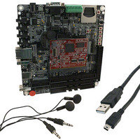
EA LPC177X/8X EVAL BOARD
Manufacturer
NXP Semiconductors
Series
-r
Type
MCUr
Specifications of OM13001,598
Contents
Board, Cable, Headphones, Registration Card
Lead Free Status / Rohs Status
Lead free / RoHS Compliant
For Use With/related Products
LPC1788
Other names
568-6707


NXP Semiconductors
Table 3.
Not all functions are available on all parts. See
pins).
LPC178X_7X
Objective data sheet
Symbol
P1[11]
P1[12]
P1[13]
P1[14]
P1[15]
P1[16]
P1[17]
P1[18]
Pin description
163 A14
157 A16
147 D16
184 A7
182 A8
180 D10
178 A9
66
P7
…continued
A12
A14
D14 -
D8
A8
B8
C9
L5
-
-
128
126
125
123
46
[3]
[3]
[3]
[3]
[3]
[3]
[3]
[3]
All information provided in this document is subject to legal disclaimers.
I;
PU
I;
PU
I;
PU
I;
PU
I;
PU
I;
PU
I;
PU
I;
PU
Table 2
Rev. 2 — 27 May 2011
I/O
I
I/O
O
I/O
I
I/O
I
I/O
I
I/O
I
-
I
I/O
I
-
I/O
I/O
O
O
I/O
I/O
O
I/O
O
O
I
-
I/O
(Ethernet, USB, LCD, QEI, SD/MMC, DAC pins) and
Description
P1[11] — General purpose digital input/output pin.
ENET_RXD2 — Ethernet Receive Data 2 (MII interface).
SD_DAT[2] — Data line 2 for SD card interface.
PWM0[6] — Pulse Width Modulator 0, output 6.
P1[12] — General purpose digital input/output pin.
ENET_RXD3 — Ethernet Receive Data (MII interface).
SD_DAT[3] — Data line 3 for SD card interface.
PWM0_CAP0 — Capture input for PWM0, channel 0.
P1[13] — General purpose digital input/output pin.
ENET_RX_DV — Ethernet Receive Data Valid (MII interface).
P1[14] — General purpose digital input/output pin.
ENET_RX_ER — Ethernet receive error (RMII/MII interface).
R — Function reserved.
T2_CAP0 — Capture input for Timer 2, channel 0.
P1[15] — General purpose digital input/output pin.
ENET_RX_CLK (ENET_REF_CLK) — Ethernet Receive Clock
(MII interface) or Ethernet Reference Clock (RMII interface).
R — Function reserved.
I2C2_SDA — I
specialized I2C pad).
P1[16] — General purpose digital input/output pin.
ENET_MDC — Ethernet MIIM clock.
I2S_TX_MCLK — I2S transmit master clock.
P1[17] — General purpose digital input/output pin.
ENET_MDIO — Ethernet MIIM data input and output.
I2S_RX_MCLK — I2S receive master clock.
P1[18] — General purpose digital input/output pin.
USB_UP_LED1 — USB port 1 GoodLink LED indicator. It is
LOW when device is configured (non-control endpoints
enabled). It is HIGH when the device is not configured or during
global suspend.
PWM1[1] — Pulse Width Modulator 1, channel 1 output.
T1_CAP0 — Capture input for Timer 1, channel 0.
R — Function reserved.
SSP1_MISO — Master In Slave Out for SSP1.
2
C2 data input/output (this pin does not use a
32-bit ARM Cortex-M3 microcontroller
LPC178x/7x
© NXP B.V. 2011. All rights reserved.
Table 7
18 of 117
(EMC
Related parts for OM13001,598
Image
Part Number
Description
Manufacturer
Datasheet
Request
R

Part Number:
Description:
NXP Semiconductors designed the LPC2420/2460 microcontroller around a 16-bit/32-bitARM7TDMI-S CPU core with real-time debug interfaces that include both JTAG andembedded trace
Manufacturer:
NXP Semiconductors
Datasheet:

Part Number:
Description:
NXP Semiconductors designed the LPC2458 microcontroller around a 16-bit/32-bitARM7TDMI-S CPU core with real-time debug interfaces that include both JTAG andembedded trace
Manufacturer:
NXP Semiconductors
Datasheet:
Part Number:
Description:
NXP Semiconductors designed the LPC2468 microcontroller around a 16-bit/32-bitARM7TDMI-S CPU core with real-time debug interfaces that include both JTAG andembedded trace
Manufacturer:
NXP Semiconductors
Datasheet:
Part Number:
Description:
NXP Semiconductors designed the LPC2470 microcontroller, powered by theARM7TDMI-S core, to be a highly integrated microcontroller for a wide range ofapplications that require advanced communications and high quality graphic displays
Manufacturer:
NXP Semiconductors
Datasheet:
Part Number:
Description:
NXP Semiconductors designed the LPC2478 microcontroller, powered by theARM7TDMI-S core, to be a highly integrated microcontroller for a wide range ofapplications that require advanced communications and high quality graphic displays
Manufacturer:
NXP Semiconductors
Datasheet:
Part Number:
Description:
The Philips Semiconductors XA (eXtended Architecture) family of 16-bit single-chip microcontrollers is powerful enough to easily handle the requirements of high performance embedded applications, yet inexpensive enough to compete in the market for hi
Manufacturer:
NXP Semiconductors
Datasheet:
Part Number:
Description:
The XA-S3 device is a member of Philips Semiconductors? XA(eXtended Architecture) family of high performance 16-bitsingle-chip microcontrollers
Manufacturer:
NXP Semiconductors
Datasheet:

Part Number:
Description:
The NXP BlueStreak LH75401/LH75411 family consists of two low-cost 16/32-bit System-on-Chip (SoC) devices
Manufacturer:
NXP Semiconductors
Datasheet:
Part Number:
Description:
The NXP LPC3130/3131 combine an 180 MHz ARM926EJ-S CPU core, high-speed USB2
Manufacturer:
NXP Semiconductors
Datasheet:
Part Number:
Description:
The NXP LPC3141 combine a 270 MHz ARM926EJ-S CPU core, High-speed USB 2
Manufacturer:
NXP Semiconductors
Part Number:
Description:
The NXP LPC3143 combine a 270 MHz ARM926EJ-S CPU core, High-speed USB 2
Manufacturer:
NXP Semiconductors

Part Number:
Description:
The NXP LPC3152 combines an 180 MHz ARM926EJ-S CPU core, High-speed USB 2
Manufacturer:
NXP Semiconductors
Part Number:
Description:
The NXP LPC3154 combines an 180 MHz ARM926EJ-S CPU core, High-speed USB 2
Manufacturer:
NXP Semiconductors