EPC9003 EPC, EPC9003 Datasheet - Page 4
EPC9003
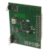
Manufacturer Part Number
EPC9003
Description
BOARD DEV FOR EPC2010 200V GAN
Manufacturer
EPC
Series
-r
Datasheet
1.EPC2010.pdf
(5 pages)
Specifications of EPC9003
Design Resources
EPC9003 Gerber Files EPC9003 Bill of Materials
Featured Product
EPC Development Tools
Main Purpose
Power Management, Half H-Bridge Driver (External FET)
Embedded
No
Utilized Ic / Part
EPC2010
Primary Attributes
200V, 5A Max Output GaNFET Capability
Secondary Attributes
GaNFET Driver Circuit Uses 7 ~ 12V
Lead Free Status / Rohs Status
Contains lead / RoHS non-compliant
Other names
917-1012


eGaN® FET DATASHEET
EPC – EFFICIENT POWER CONVERSION CORPORATION | WWW.EPC-CO.COM | COPYRIGHT 2011 |
DIE MARKINGS
TAPE AND REEL CONFIGURATION
4mm pitch, 8mm wide tape on 7” reel
7” reel
Figure 11: Transient Thermal Response Curve
0.0001
0.001
0.01
0.1
1
10
Gate Pad solder bar
is under this corner
Die orientation dot
Duty Factors:
0.5
0.2
0.1
0.05
0.02
0.01
-5
a
Dimension (mm)
b
c (note 2)
f (note 2)
c
a
b
d
e
g
10
-4
Single Pulse
d
target
8.00
1.75
3.50
4.00
4.00
2.00
1.5
EPC2010 (note 1)
Normalized Maximum Transient Thermal Impedance
10
min
1.65
3.45
3.90
3.90
1.95
7.90
-3
1.5
e
2010
YYYY
ZZZZ
t
p
, Rectangular Pulse Duration, seconds
8.30
max
1.85
3.55
4.10
4.10
2.05
1.6
10
f
Note 1: MSL1 (moisture sensitivity level 1) classi ed according to IPC/JEDEC industry standard.
Note 2: Pocket position is relative to the sprocket hole measured as true position of the pocket,
-2
not the pocket hole.
EPC2010
Number
g
Part
10
-1
Notes:
Duty Factor: D = t
Peak T
Marking Line 1
Loaded Tape Feed Direction
J
= P
Part #
2010
1
DM
Die is placed into pocket
P
x Z
solder bar side down
DM
θJB
(face side down)
1
/t
x R
Laser Markings
Lot_Date Code
Marking line 2
2
t
θJB
1
10
YYYY
+ T
t
2
B
Lot_Date Code
Marking Line 3
100
solder bar is
orientation
under this
ZZZZ
corner
Gate
dot
Die
EPC2010
| PAGE 4
Related parts for EPC9003
Image
Part Number
Description
Manufacturer
Datasheet
Request
R

Part Number:
Description:
Multi Video Capture Ports Embedded PC
Manufacturer:
PROTECHSYSTEMS [Protech Systems Co., Ltd.]
Datasheet:

Part Number:
Description:
IC CONFIG DEVICE 1MBIT 8-DIP
Manufacturer:
Altera
Datasheet:

Part Number:
Description:
IC CONFIG DEVICE 1.6MBIT 20-PLCC
Manufacturer:
Altera
Datasheet:
Part Number:
Description:
IC CONFIG DEVICE 1.6MBIT 20-PLCC
Manufacturer:
Altera
Datasheet:

Part Number:
Description:
IC CONFIG DEVICE 1.6MBIT 32-TQFP
Manufacturer:
Altera
Datasheet:
Part Number:
Description:
IC CONFIG DEVICE 1.6MBIT 32-TQFP
Manufacturer:
Altera
Datasheet:
Part Number:
Description:
IC CONFIG DEVICE 1.6MBIT 20-PLCC
Manufacturer:
Altera
Datasheet:
Part Number:
Description:
IC CONFIG DEVICE 1.6MBIT 20-PLCC
Manufacturer:
Altera
Datasheet:

Part Number:
Description:
IC CONFIG DEVICE 8MBIT 100-PQFP
Manufacturer:
Altera
Datasheet:
Part Number:
Description:
IC CONFIG DEVICE 1.6MBIT 32-TQFP
Manufacturer:
Altera
Datasheet:
Part Number:
Description:
IC CONFIG DEVICE 1.6MBIT 32-TQFP
Manufacturer:
Altera
Datasheet:
Part Number:
Description:
IC CONFIG DEVICE 16MBIT 100-PQFP
Manufacturer:
Altera
Datasheet:
Part Number:
Description:
IC CONFIG DEVICE 16MBIT 100-PQFP
Manufacturer:
Altera
Datasheet:
Part Number:
Description:
IC CONFIG DEVICE 16MBIT 100-PQFP
Manufacturer:
Altera
Datasheet:

Part Number:
Description:
IC CONFIG DEVICE 16MBIT 88-UBGA
Manufacturer:
Altera
Datasheet: