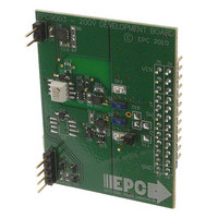
EPC9003 EPC, EPC9003 Datasheet

BOARD DEV FOR EPC2010 200V GAN

EPC9003

Manufacturer Part Number
EPC9003
Description
BOARD DEV FOR EPC2010 200V GAN
Manufacturer
EPC
Series
-r
Datasheet

Specifications of EPC9003

Design Resources
EPC9003 Gerber Files EPC9003 Bill of Materials
Featured Product
EPC Development Tools
Main Purpose
Power Management, Half H-Bridge Driver (External FET)
Embedded
No
Utilized Ic / Part
EPC2010
Primary Attributes
200V, 5A Max Output GaNFET Capability
Secondary Attributes
GaNFET Driver Circuit Uses 7 ~ 12V
Lead Free Status / Rohs Status
Contains lead / RoHS non-compliant
Other names
917-1012
eGaN® FET DATASHEET
V
R
I
EPC – EFFICIENT POWER CONVERSION CORPORATION | WWW.EPC-CO.COM | COPYRIGHT 2011 |
EPC2010 – Enhancement Mode Power Transistor
Gallium Nitride is grown on Silicon Wafers and processed using standard CMOS equipment leverag-
ing the infrastructure that has been developed over the last 55 years. GaN’s exceptionally high elec-
tron mobility and low temperature coefficient allows very low R
and majority carrier diode provide exceptionally low Q
can handle tasks where very high switching frequency, and low on-time are beneficial as well as
those where on-state losses dominate.
Note 1: R
D
Static Characteristics (T
Source-Drain Characteristics (T
Dynamic Characteristics (T
DSS
DS(ON)
, 12 A
T
V
V
T
I
STG
DS
D
See http://epc-co.com/epc/documents/product-training/Appnote_Thermal_Performance_of_eGaN_FETs.pdf for details.
, 200 V
GS
R
J
V
BV
θ
JA
C
C
Q
Q
I
I
DS(ON)
V
C
GS(TH)
Q
DSS
GSS
R
R
R
is determined with the device mounted on one square inch of copper pad, single layer 2 oz copper on FR4 board.
OSS
RSS
, 25 mW
SD
ISS
GD
DSS
GS
G
θ JC
θ JB
θ JA
Drain-to-Source Voltage
Continuous (T
Pulsed (25˚C, Tpulse = 300 µs)
Gate-to-Source Voltage
Operating Temperature
Storage Temperature
Gate-Source Forward Leakage
Source-Drain Forward Voltage
PARAMETER
Gate-Source Reverse Leakage
PARAMETER
Reverse Transfer Capacitance
Drain-Source On Resistance
Total Gate Charge (V
Thermal Resistance, Junction to Case
Thermal Resistance, Junction to Board
Thermal Resistance, Junction to Ambient (Note 1)
Drain-to-Source Voltage
Gate Threshold Voltage
Gate to Source Charge
J
Drain Source Leakage
Gate to Drain Charge
= 25˚C unless otherwise stated)
Output Capacitance
A
Input Capacitance
=25˚C, θ
J
= 25˚C unless otherwise stated)
J
= 25˚C unless otherwise stated)
JA
= 13)
Maximum Ratings
GS
PRELIMINARY
= 5 V)
G
and zero Q
I
S
I
S
= 0.5 A, V
= 0.5 A, V
DS(ON)
Thermal Characteristics
V
V
V
V
V
-40 to 125
-40 to 150
GS
DS
DS
DS
DS
V
TEST CONDITIONS
TEST CONDITIONS
GS
= 0 V, I
= V
= 100 V, I
= 160 V, V
= 100 V, V
, while its lateral device structure
RR
200
12
60
-5
6
= 5 V, I
. The end result is a device that
V
V
GS
GS
GS
GS
GS
, I
= -5 V
= 0 V, T = 125˚C
= 5 V
= 0 V, T = 25˚C
D
D
= 200 µA
= 3 mA
D
D
GS
= 6 A
GS
= 12 A
= 0 V
= 0 V
˚C
V
A
V
MIN
200
MIN
0.7
EFFICIENT POWER CONVERSION
EPC2010 eGaN® FETs are supplied only in
passivated die form with solder bars
Applications
• High Speed DC-DC conversion
• Class D Audio
• Hard Switched and High Frequency Circuits
Benefits
• Ultra High Efficiency
• Ultra Low R
• Ultra low Q
• Ultra small footprint
TYP
TYP
480
270
0.2
1.4
1.8
1.8
1.7
1.3
50
18
11
5
1
1.8
TYP
16
56
G
DS(on)
MAX
MAX
150
2.5
7.5
2.6
25
3
1
2
HAL
˚C/W
˚C/W
˚C/W
EPC2010
| PAGE 1
UNIT
UNIT
mA
µA
pF
nC
V
V
V

Related parts for EPC9003

EPC9003 Summary of contents

Page 1

... FR4 board. JA θ Q Total Gate Charge (V See http://epc-co.com/epc/documents/product-training/Appnote_Thermal_Performance_of_eGaN_FETs.pdf for details Gate to Drain Charge GD EPC – EFFICIENT POWER CONVERSION CORPORATION | WWW.EPC-CO.COM | COPYRIGHT 2011 | Q Gate to Source Charge GS PRELIMINARY , while its lateral device structure DS(ON) and zero Q . The end result is a device that G ...

Page 2

... V – Drain to Source Voltage (V) DS Figure for Various Current DS(ON 2 – Gate to Source Voltage (V) GS EPC – EFFICIENT POWER CONVERSION CORPORATION | WWW.EPC-CO.COM | COPYRIGHT 2011 | 25˚ 0 125˚ TEST CONDITIONS V = 100 100 2 4.5 5 5.5 1.8 1.8 MIN ...

Page 3

... Figure 7: Reverse Drain-Source Characteristics 60 25˚C 125˚ 0.5 1 1.5 2 2.5 V – Source to Drain Voltage (V) SD Figure 9: Normalized Threshold Voltage vs Temperature - – Junction Temperature ( ˚ EPC – EFFICIENT POWER CONVERSION CORPORATION | WWW.EPC-CO.COM | COPYRIGHT 2011 | OSS ISS RSS 150 200 3 3.5 4 4.5 -20 .03 ...

Page 4

... Dimension (mm) c (note 2) f (note 2) DIE MARKINGS Die orientation dot Gate Pad solder bar is under this corner EPC – EFFICIENT POWER CONVERSION CORPORATION | WWW.EPC-CO.COM | COPYRIGHT 2011 | Normalized Maximum Transient Thermal Impedance Single Pulse Rectangular Pulse Duration, seconds ...

Page 5

... FET DATASHEET DIE OUTLINE f Solder Bar View Side View RECOMMENDED LAND PATTERN 1 (units in µm) 2 EPC – EFFICIENT POWER CONVERSION CORPORATION | WWW.EPC-CO.COM | COPYRIGHT 2011 | SEATING PLANE 600 600 X4 3554 250 250 X5 MICROMETERS DIM MIN Nominal A 3524 3554 7 B 1602 1632 ...

Related keywords