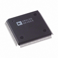
AD9887KS-100 Analog Devices Inc, AD9887KS-100 Datasheet - Page 9

AD9887KS-100
Manufacturer Part Number
AD9887KS-100
Description
IC INTRFACE ANALOG/DVI 160-MQFP
Manufacturer
Analog Devices Inc
Datasheet
1.AD9887AKSZ-100.pdf
(40 pages)
Specifications of AD9887KS-100
Rohs Status
RoHS non-compliant
Applications
Graphic Cards, VGA Interfaces
Interface
Analog and Digital
Voltage - Supply
3.15 V ~ 3.45 V
Package / Case
160-MQFP, 160-PQFP
Mounting Type
Surface Mount
Pin Type
Analog Video Inputs
External
Sync/Clock
Inputs
Sync Outputs
Voltage Reference
Clamp Voltages
PLL Filter
Power Supply
PIN FUNCTION DETAILS (ANALOG INTERFACE)
Inputs
R
G
B
HSYNC
AIN
AIN
AIN
Analog Input for RED Channel
Analog Input for GREEN Channel
Analog Input for BLUE Channel
High-impedance inputs that accept the RED,
GREEN, and BLUE channel graphics signals,
respectively. For RGB, the three channels are
identical and can be used for any colors, but
colors are assigned for convenient reference.
For proper 4:2:2 formatting in a YUV appli-
cation, the Y channel must be connected to
the G
B
R
They accommodate input signals ranging
from 0.5 V to 1.0 V full scale. Signals should
be ac-coupled to these pins to support clamp
operation.
Horizontal Sync Input
This input receives a logic signal that estab-
lishes the horizontal timing reference and
provides the frequency reference for pixel
clock generation.
The logic sense of this pin is controlled by
serial register 0Fh Bit 7 (HSYNC Polarity).
Only the leading edge of HSYNC is active,
the trailing edge is ignored. When HSYNC
AIN
AIN
Pin Name
R
G
B
HSYNC
VSYNC
SOGIN
CLAMP
COAST
CKEXT
CKINV
HSOUT
VSOUT
SOGOUT
REFOUT
REFIN
R
R
G
G
B
B
FILT
V
PV
V
GND
input, and V must be connected to the
input.
AIN
AIN
AIN
MIDSC
CLAMP
MIDSC
CLAMP
D
DD
AIN
MIDSC
CLAMP
D
input, U must be connected to the
V
V
V
V
V
V
Function
Analog Input for Converter R
Analog Input for Converter G
Analog Input for Converter B
Horizontal SYNC Input
Vertical SYNC Input
Sync-on-Green Input
Clamp Input (External CLAMP Signal)
PLL COAST Signal Input
External Pixel Clock Input (to Bypass Internal PLL)
or 10 kΩ to V
ADC Sampling Clock Invert
HSYNC Output (Phase-Aligned with DATACK and DATACK)
VSYNC Output (Asynchronous)
Sync-on-Green Slicer Output or Raw HSYNC Output
Internal Reference Output (bypass with 0.1 µF to ground)
Reference Input (1.25 V ± 10%)
Voltage output equal to the RED converter midscale voltage.
During midscale clamping, the RED Input is clamped to this pin.
Voltage output equal to the GREEN converter midscale voltage.
During midscale clamping, the GREEN Input is clamped to this pin.
Voltage output equal to the BLUE converter midscale voltage.
During midscale clamping, the BLUE Input is clamped to this pin.
Connection for External Filter Components for Internal PLL
Main Power Supply
PLL Power Supply (Nominally 3.3 V)
Output Power Supply
Ground
Table II. Analog Interface Pin List
DD
VSYNC
SOGIN
Polarity = 0, the falling edge of HSYNC is
used. When HSYNC Polarity = 1, the rising
edge is active.
The input includes a Schmitt trigger for noise
immunity, with a nominal input threshold
of 1.5 V.
Electrostatic Discharge (ESD) protection
diodes will conduct heavily if this pin is driven
more than 0.5 V above the maximum toler-
ance voltage (3.3 V), or more than 0.5 V
below ground.
Vertical Sync Input
This is the input for vertical sync.
Sync-on-Green Input
This input is provided to assist with processing
signals with embedded sync, typically on the
GREEN channel. The pin is connected to a
high-speed comparator with an internally
generated threshold, which is set to 0.15 V
above the negative peak of the input signal.
When connected to an ac-coupled graphics
signal with embedded sync, it will produce a
noninverting digital output on SOGOUT.
When not used, this input should be left
unconnected. For more details on this func-
tion and how it should be configured, refer to
the Sync-on-Green section.
Value
0.0 V to 1.0 V
0.0 V to 1.0 V
0.0 V to 1.0 V
3.3 V CMOS
3.3 V CMOS
0.0 V to 1.0 V
3.3 V CMOS
3.3 V CMOS
3.3 V CMOS
3.3 V CMOS
3.3 V CMOS
3.3 V CMOS
3.3 V CMOS
1.25 V
1.25 V ± 10%
0.5 V ± 50%
0.0 V to 0.75 V
0.5 V ± 50%
0.0 V to 0.75 V
0.5 V ± 50%
0.0 V to 0.75 V
3.3 V ± 5%
3.3 V ± 5%
3.3 V or 2.5 V ± 5%
0 V
AD9887
82
93
83
Pin No.
119
110
100
81
108
84
94
139
138
140
126
125
120
118
111
109
101
99
78


