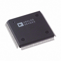
AD9887KS-100 Analog Devices Inc, AD9887KS-100 Datasheet - Page 17

AD9887KS-100
Manufacturer Part Number
AD9887KS-100
Description
IC INTRFACE ANALOG/DVI 160-MQFP
Manufacturer
Analog Devices Inc
Datasheet
1.AD9887AKSZ-100.pdf
(40 pages)
Specifications of AD9887KS-100
Rohs Status
RoHS non-compliant
Applications
Graphic Cards, VGA Interfaces
Interface
Analog and Digital
Voltage - Supply
3.15 V ~ 3.45 V
Package / Case
160-MQFP, 160-PQFP
Mounting Type
Surface Mount
SCAN Function
The SCAN function is intended as a pseudo JTAG function for
manufacturing test of the board. The ordinary operation of the
AD9887 is disabled during SCAN.
To enable the SCAN function, set register 14h, bit 2 to 1. To
SCAN in data to all 48 digital outputs, apply 48 serial bits of
data and 48 clocks (typically 5 MHz, max of 20 MHz) to the
SCAN
in on the rising edge of SCAN
in will appear at the RED A<7> output after one clock cycle.
After 48 clocks, the first bit is shifted all the way to the BLU
B<0>. The 48th bit will now be at the RED A<7> output. If
SCAN
shifted from RED A<7> to BLU B<0> and will come out of the
SCAN
This is illustrated in Figure 10. A setup time (t
should be plenty and no hold time (t
This is illustrated in Figure 11.
CLK
IN
OUT
and SCAN
IN
continues after 48 cycles, the data will continue to be
pin as serial data on the falling edge of SCAN
CLAMP
OFFSET
V
(128 CODES)
DAC
OFF
7
CLK
BLUE B<0>
0.5V
SCANOUT
SCANCLK
RED A<7>
0V
SCANIN
V
pins respectively. The data is shifted
OFF
x1.2
CLK
BIT 1
. The first serial bit shifted
X
HOLD
BIT 1
V
(128 CODES)
GAIN
DAC
ADC
X
OFF
) is required (≥ 0 ns).
8
BIT 2
1V
0V
X
8
REF
BIT 2
SU
X
) of 3 ns
BIT 3
X
BIT 3
X
CLK
.
BIT 46
X
Alternate Pixel Sampling Mode
A Logic 1 input on Clock Invert (CKINV, Pin 94) inverts the
nominal ADC clock. CKINV can be switched between frames
to implement the alternate pixel sampling mode. This allows
higher effective image resolution to be achieved at lower pixel
rates but with lower frame rates.
On one frame, only even pixels are digitized. On the subsequent
frame, odd pixels are sampled. By reconstructing the entire
frame in the graphics controller, a complete image can be recon-
structed. This is very similar to the interlacing process that is
employed in broadcast television systems, but the interlacing is
vertical instead of horizontal. The frame data is still presented to
the display at the full desired refresh rate (usually 60 Hz) so no
flicker artifacts are added.
BIT 47
SCANCLK
SCANIN
X
BIT 47
X
BIT 48
X
BIT 48
BIT 1
O
O
O
O
O
O
O
O
O
O
O
O 1
O 1
O 1
O 1
O 1
O 1
O 1
O 1
O 1
O 1
O 1
t
SU
E
E
E
E
E
E
E
E
E
E
E
= 3ns
BIT 1
X
O 1
O 1
O 1
O 1
O 1
O 1
O 1
O 1
O 1
O 1
O 1
O
O
O
O
O
O
O
O
O
O
O
E
E
E
E
E
E
E
E
E
E
E
BIT 2
X
O 1
O 1
O 1
O 1
O 1
O 1
O 1
O 1
O 1
O 1
O 1
O
O
O
O
O
O
O
O
O
O
O
BIT 2
E
E
E
E
E
E
E
E
E
E
E
O 1
O 1
O 1
O 1
O 1
O 1
O 1
O 1
O 1
O 1
O 1
O
O
O
O
O
O
O
O
O
O
O
t
HOLD
E
E
E
E
E
E
E
E
E
E
E
O 1
O 1
O 1
O 1
O 1
O 1
O 1
O 1
O 1
O 1
O 1
= 0ns
O
O
O
O
O
O
O
O
O
O
O
E
E
E
E
E
E
E
E
E
E
E
O 1
O 1
O 1
O 1
O 1
O 1
O 1
O 1
O 1
O 1
O 1
O
O
O
O
O
O
O
O
O
O
O
E
E
E
E
E
E
E
E
E
E
E
AD9887


