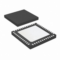
DS08MB200TSQX/NOPB National Semiconductor, DS08MB200TSQX/NOPB Datasheet - Page 7

DS08MB200TSQX/NOPB
Manufacturer Part Number
DS08MB200TSQX/NOPB
Description
IC MUX/BUFFER DUAL 800MBPS 48LLP
Manufacturer
National Semiconductor
Type
MUXr
Datasheet
1.DS08MB200TSQNOPB.pdf
(10 pages)
Specifications of DS08MB200TSQX/NOPB
Tx/rx Type
LVDS
Delay Time
1.0ns
Capacitance - Input
3.5pF
Voltage - Supply
3 V ~ 3.6 V
Current - Supply
275mA
Mounting Type
Surface Mount
Package / Case
48-LLP
Number Of Elements
3
Number Of Receivers
3
Number Of Drivers
3
Input Type
CMOS/TTL
Operating Supply Voltage (typ)
3.3V
Differential Input High Threshold Voltage
100mV
Diff. Input Low Threshold Volt
-100mV
Output Type
Repeater
Differential Output Voltage
500mV
Transmission Data Rate
800Mbps
Propagation Delay Time
2.5ns
Power Dissipation
5.2W
Operating Temp Range
-40C to 85C
Operating Temperature Classification
Industrial
Mounting
Surface Mount
Pin Count
48
Package Type
LLP
Lead Free Status / RoHS Status
Lead free / RoHS Compliant
Other names
*DS08MB200TSQX/NOPB
DS08MB200TSQX
DS08MB200TSQX
Interfacing LVPECL to LVDS
An LVPECL driver consists of a differential pair with coupled
emitters connected to GND via a current source. This drives
a pair of emitter-followers that require a 50 ohm to V
load. A modern LVPECL driver will typically include the ter-
mination scheme within the device for the emitter follower. If
the driver does not include the load, then an external scheme
must be used. The 1.3 V supply is usually not readily available
on a PCB, therefore, a load scheme without a unique power
supply requirement may be used.
Figure 2 is a separated π termination scheme for a 3.3 V
LVPECL driver. R1 and R2 provides proper DC load for the
driver emitter followers, and may be included as part of the
driver device (Note 16). The DS08MB200 includes a 100 ohm
input termination for the transmission line. The common mode
voltage will be at the normal LVPECL levels – around 2 V.
This scheme works well with LVDS receivers that have rail-
to-rail common mode voltage, V
Semiconductor LVDS receivers have wide V
exceptions are noted in devices’ respective datasheets.
Those LVDS devices that do have a wide V
vary in performance significantly when receiving a signal with
a common mode other than standard LVDS V
An AC coupled interface is preferred when transmitter and
receiver ground references differ more than 1 V. This is a
likely scenario when transmitter and receiver devices are on
separate PCBs. Figure 3 illustrates an AC coupled interface
between a LVPECL driver and LVDS receiver. R1 and R2, if
not present in the driver device (Note 16), provide DC load for
the emitter followers and may range between 140-220 ohms
for most LVPECL devices for this particular configuration. The
DS08MB200 includes an internal 100 ohm resistor to termi-
nate the transmission line for minimal reflections. The signal
after ac coupling capacitors will swing around a level set by
internal biasing resistors (i.e. fail-safe) which is either V
or 0 V depending on the actual failsafe implementation. If in-
ternal biasing is not implemented, the signal common mode
voltage will slowly wander to GND level.
FIGURE 2. DC Coupled LVPECL to LVDS Interface
FIGURE 3. AC Coupled LVPECL to LVDS Interface
CM
, range. Most National
CM
CM
CM
range do not
of 1.2 V.
range. The
20157461
20157462
CC
DD
-2.0
/2
7
Interfacing LVDS to LVPECL
An LVDS driver consists of a current source (nominal 3.5mA)
which drives a CMOS differential pair. It needs a differential
resistive load in the range of 70 to 130 ohms to generate
LVDS levels. In a system, the load should be selected to
match transmission line characteristic differential impedance
so that the line is properly terminated. The termination resistor
should be placed as close to the receiver inputs as possible.
When interfacing an LVDS driver with a non-LVDS receiver,
one only needs to bias the LVDS signal so that it is within the
common mode range of the receiver. This may be done by
using separate biasing voltage which demands another pow-
er supply. Some receivers have required biasing voltage
available on-chip (V
Figure 4 illustrates interface between an LVDS driver and a
LVPECL with a V
the receiver (Note 16), provide proper resistive load for the
driver and termination for the transmission line, and V
desired bias for the receiver.
Figure 5 illustrates AC coupled interface between an LVDS
driver and LVPECL receiver without a V
resistors R1, R2, R3, and R4, if not present in the receiver
(Note 16), provide a load for the driver, terminate the trans-
mission line, and bias the signal for the receiver.
Note 16: The bias networks shown above for LVPECL drivers and receivers
may or may not be present within the driver device. The LVPECL driver and
receiver specification must be reviewed closely to ensure compatibility
between the driver and receiver terminations and common mode operating
ranges.
FIGURE 4. DC Coupled LVDS to LVPECL Interface
FIGURE 5. AC Coupled LVDS to LVPECL Interface
T
pin available. R1 and R2, if not present in
T
, V
TT
or V
BB
).
T
pin available. The
www.national.com
20157464
20157463
T
sets


