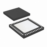
DS08MB200TSQX/NOPB National Semiconductor, DS08MB200TSQX/NOPB Datasheet - Page 4

DS08MB200TSQX/NOPB
Manufacturer Part Number
DS08MB200TSQX/NOPB
Description
IC MUX/BUFFER DUAL 800MBPS 48LLP
Manufacturer
National Semiconductor
Type
MUXr
Datasheet
1.DS08MB200TSQNOPB.pdf
(10 pages)
Specifications of DS08MB200TSQX/NOPB
Tx/rx Type
LVDS
Delay Time
1.0ns
Capacitance - Input
3.5pF
Voltage - Supply
3 V ~ 3.6 V
Current - Supply
275mA
Mounting Type
Surface Mount
Package / Case
48-LLP
Number Of Elements
3
Number Of Receivers
3
Number Of Drivers
3
Input Type
CMOS/TTL
Operating Supply Voltage (typ)
3.3V
Differential Input High Threshold Voltage
100mV
Diff. Input Low Threshold Volt
-100mV
Output Type
Repeater
Differential Output Voltage
500mV
Transmission Data Rate
800Mbps
Propagation Delay Time
2.5ns
Power Dissipation
5.2W
Operating Temp Range
-40C to 85C
Operating Temperature Classification
Industrial
Mounting
Surface Mount
Pin Count
48
Package Type
LLP
Lead Free Status / RoHS Status
Lead free / RoHS Compliant
Other names
*DS08MB200TSQX/NOPB
DS08MB200TSQX
DS08MB200TSQX
www.national.com
LVTTL DC SPECIFICATIONS (MUX_Sn, ENA_n, ENB_n, ENL_n)
V
V
I
I
C
C
V
LVDS INPUT DC SPECIFICATIONS (SIA±, SIB±, LI±)
V
V
V
V
C
I
LVDS OUTPUT DC SPECIFICATIONS (SOA_n±, SOB_n±, LO_n±)
V
ΔV
V
ΔV
I
C
Symbol
IH
IL
IN
OS
IH
IL
CL
TH
TL
ID
CMR
OD
OS
IN1
OUT1
IN2
OUT2
Absolute Maximum Ratings
Electrical Characteristics
Over recommended operating supply and temperature ranges unless other specified.
Supply Voltage (V
CMOS Input Voltage
LVDS Receiver Input Voltage (Note
7)
LVDS Driver Output Voltage
LVDS Output Short Circuit Current
Junction Temperature
Storage Temperature
Lead Temperature (Solder, 4sec)
Max Pkg Power Capacity @ 25°C
Thermal Resistance (θ
Package Derating above +25°C
ESD Last Passing Voltage
OD
OS
HBM, 1.5kΩ, 100pF
LVDS pins to GND only
High Level Input Voltage
Low Level Input Voltage
High Level Input Current
Low Level Input Current
Input Capacitance
Output Capacitance
Input Clamp Voltage
Differential Input High Threshold
(Note 9)
Differential Input Low Threshold
(Note 9)
Differential Input Voltage
Common Mode Voltage Range
Input Capacitance
Input Current
Differential Output Voltage,
(Note 9)
Change in V
Complementary States
Offset Voltage (Note 10)
Change in V
Complementary States
Output Short Circuit Current
Output Capacitance
DD
)
Parameter
OD
OS
JA
between
between
)
-0.3V to (V
-0.3V to (V
-0.3V to (V
−65°C to +150°C
−0.3V to +4.0V
V
V
Any Digital Input Pin to V
Any Digital Output Pin to V
I
V
V
V
V
V
V
IN+ or IN− to V
V
V
R
and OUT−
OUT+ or OUT− Short to GND
OUT+ or OUT− to GND when TRI-
STATE
CL
IN
IN
CM
DD
CM
DD
CM
ID
IN
IN
L
(Note 6)
41.7mW/°C
is the internal 100Ω between OUT+
= −18 mA
= V
= V
= 150 mV, V
= 3.6V, V
= 0V, V
= 3.6V
= 3.6V
= 0.8V or 1.2V or 3.55V,
= 0.8V or 1.2V or 3.55V,
= 0.8V to 3.55V, V
DD
DD
DD
+40 mA
24°C/W
+150°C
DD
SS
+0.3V)
+0.3V)
+0.3V)
260°C
5.2W
15kV
, V
= V
8kV
DD
DD
DD
DDMAX
= V
Conditions
= V
SS
= V
DD
DDMAX
4
DDMAX
= 3.6V
DDMAX
Recommended Operating
Conditions
Note 6: Absolute maximum ratings are those values beyond which damage
to the device may occur. The databook specifications should be met, without
exception, to ensure that the system design is reliable over its power supply,
temperature, and output/input loading variables. National does not
recommend operation of products outside of recommended operation
conditions.
Note 7: V
DD
Supply Voltage (V
Input Voltage (V
Output Voltage (V
Operating Temperature (T
SS
EIAJ, 0Ω, 200pF
CDM
Industrial
= 3.6V
SS
ID
max < 2.4V
I
) (Note 7)
O
CC
)
)
GND
−100
−1.5
0.05
1.05
Min
−10
−10
100
−15
−15
250
-35
-35
2.0
A
)
(Note 8)
−0.8
1.22
Typ
360
−21
3.5
5.5
3.5
5.5
0
0
−40°C to +85°C
1.475
2400
Max
3.55
V
+10
+10
100
+15
+15
500
0.8
-40
35
35
3.0V to 3.6V
DD
0V to V
0V to V
1000V
250V
Units
mV
mV
mV
mV
mV
mV
mA
µA
µA
µA
µA
CC
CC
pF
pF
pF
pF
V
V
V
V
V


