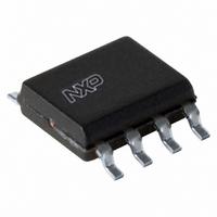
PCA9510AD,112 NXP Semiconductors, PCA9510AD,112 Datasheet - Page 7

PCA9510AD,112
Manufacturer Part Number
PCA9510AD,112
Description
IC I2C/SMBUS BUFF 8-SOIC
Manufacturer
NXP Semiconductors
Type
Bufferr
Datasheet
1.PCA9510ADP118.pdf
(24 pages)
Specifications of PCA9510AD,112
Tx/rx Type
I²C Logic
Delay Time
35ns
Capacitance - Input
1.9pF
Voltage - Supply
2.7 V ~ 5.5 V
Current - Supply
6mA
Mounting Type
Surface Mount
Package / Case
8-SOIC (3.9mm Width)
Maximum Operating Temperature
+ 85 C
Mounting Style
SMD/SMT
Minimum Operating Temperature
- 40 C
Lead Free Status / RoHS Status
Lead free / RoHS Compliant
Other names
568-3357-5
935280025112
PCA9510AD
935280025112
PCA9510AD
NXP Semiconductors
PCA9510A_4
Product data sheet
8.4 Propagation delays
8.5 READY digital output
8.6 ENABLE low current disable
8.7 Resistor pull-up value selection
The delay for a rising edge is determined by the combined pull-up current from the bus
resistors and the rise time accelerator current source and the effective capacitance on the
lines. If the pull-up currents are the same, any difference in rise time is directly
proportional to the difference in capacitance between the two sides. The t
negative if the output capacitance is less than the input capacitance and would be positive
if the output capacitance is larger than the input capacitance, when the currents are the
same.
The t
below 0.7V
maximum slew rate, and even if the input slew rate is slow enough that the output catches
up it will still lag the falling voltage of the input by the offset voltage. The maximum t
occurs when the input is driven LOW with zero delay and the output is still limited by its
turn-on delay and the falling edge slew rate. The output falling edge slew rate is a function
of the internal maximum slew rate which is a function of temperature, V
well as the load current and the load capacitance.
This pin provides a digital flag which is LOW when either ENABLE is LOW or the start-up
sequence described earlier in this section has not been completed. READY goes HIGH
when ENABLE is HIGH and start-up is complete. The pin is driven by an open-drain
pull-down capable of sinking 3 mA while holding 0.4 V on the pin. Connect a resistor of
10 k to V
Grounding the ENABLE pin disconnects the backplane side from the card side, disables
the rise time accelerators, drives READY LOW, disables the bus precharge circuitry, and
puts the part in a low current state. When the pin voltage is driven all the way to V
part waits for data transactions on both the backplane and card sides to be complete
before reconnecting the two sides.
The system pull-up resistors must be strong enough to provide a positive slew rate of
1.25 V/ s on the SDAn and SCLn pins, in order to activate the boost pull-up currents
during rising edges. Choose maximum resistor value using
where R
volts, and C is the equivalent bus capacitance in picofarads.
In addition, regardless of the bus capacitance, always choose R
V
requires logic HIGH voltages on SDAOUT and SCLOUT to connect the backplane to the
card, and these pull-up values are needed to overcome the precharge voltage. See the
curves in
R
CC
PU
= 5.5 V maximum, R
PHL
800 10
PU
can never be negative because the output does not start to fall until the input is
Figure 5
CC
CC
is the pull-up resistor value in ohms, V
, and the output turn on has a non-zero delay, and the output has a limited
to provide the pull-up.
3
V
---------------------------------- -
and
CC min
Rev. 04 — 18 August 2009
Figure 6
C
PU
–
0.6
45 k for V
for guidance in resistor pull-up selection.
Hot swappable I
CC
= 3.6 V maximum. The start-up circuitry
CC(min)
is the minimum V
2
C-bus and SMBus bus buffer
Equation
PU
PCA9510A
65.7 k for
1:
CC
© NXP B.V. 2009. All rights reserved.
and process, as
PLH
CC
voltage in
may be
CC
PHL
7 of 24
, the
(1)


