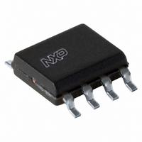
PCA9510AD,112 NXP Semiconductors, PCA9510AD,112 Datasheet - Page 5

PCA9510AD,112
Manufacturer Part Number
PCA9510AD,112
Description
IC I2C/SMBUS BUFF 8-SOIC
Manufacturer
NXP Semiconductors
Type
Bufferr
Datasheet
1.PCA9510ADP118.pdf
(24 pages)
Specifications of PCA9510AD,112
Tx/rx Type
I²C Logic
Delay Time
35ns
Capacitance - Input
1.9pF
Voltage - Supply
2.7 V ~ 5.5 V
Current - Supply
6mA
Mounting Type
Surface Mount
Package / Case
8-SOIC (3.9mm Width)
Maximum Operating Temperature
+ 85 C
Mounting Style
SMD/SMT
Minimum Operating Temperature
- 40 C
Lead Free Status / RoHS Status
Lead free / RoHS Compliant
Other names
568-3357-5
935280025112
PCA9510AD
935280025112
PCA9510AD
NXP Semiconductors
8. Functional description
PCA9510A_4
Product data sheet
8.1 Start-up
8.2 Connect circuitry
Refer to
An undervoltage and initialization circuit holds the parts in a disconnected state which
presents high-impedance to all SDAn and SCLn pins during power-up. A LOW on the
ENABLE pin also forces the parts into the low current disconnected state when the I
essentially zero. As the power supply is brought up and the ENABLE is HIGH or the part is
powered and the ENABLE is taken from LOW to HIGH, it enters an initialization state
where the internal references are stabilized and the precharge circuit is enabled. At the
end of the initialization state the ‘Stop Bit And Bus Idle’ detect circuit is enabled. With the
ENABLE pin HIGH long enough to complete the initialization state (t
HIGH when all the SDAn and SCLn pins have been HIGH for the bus idle time or when all
pins are HIGH and a STOP condition is seen on the SDAIN and SCLIN pins, SDAIN is
connected to SDAOUT and SCLIN is connected to SCLOUT. The 1 V precharge circuitry
is activated during the initialization and is deactivated when the connection is made. The
precharge circuitry pulls up the SDAIN and SCLIN input pins to 1 V through individual
100 k nominal resistors. This precharges the pins to 1 V to minimize the worst case
disturbances that result from inserting a card into the backplane where the backplane and
the card are at opposite logic levels.
Once the connection circuitry is activated, the behavior of SDAIN and SDAOUT as well as
SCLIN and SCLOUT become identical with each acting as a bidirectional buffer that
isolates the input capacitance from the output bus capacitance while communicating the
logic levels. A LOW forced on either SDAIN or SDAOUT will cause the other pin to be
driven to a LOW by the part. The same is also true for the SCLn pins. Noise between
0.7V
falls below 0.7V
one pin, the other pin in the pair turns on a pull-down driver that is referenced to a small
voltage above the falling pin. The driver will pull the pin down at a slew rate determined by
the driver and the load initially, because it does not start until the first falling pin is below
0.7V
pull-down slew rate then the initial pull-down rate will continue. If the first falling pin has a
slow slew rate then the second pin will be pulled down at its initial slew rate only until it is
just above the first pin voltage then they will both continue down at the slew rate of the
first.
Once both sides are LOW they will remain LOW until all the external drivers have stopped
driving LOWs. If both sides are being driven LOW to the same value for instance, 10 mV
by external drivers, which is the case for clock stretching and is typically the case for
acknowledge, and one side external driver stops driving that pin will rise until the internal
driver pulls it down to the offset voltage. When the last external driver stops driving a
LOW, that pin will rise up and settle out just above the other pin as both rise together with
a slew rate determined by the internal slew rate control and the RC time constant. As long
as the slew rate is at least 1.25 V/ s, when the pin voltage exceeds 0.6 V for the
PCA9510A, the pull-down driver is turned off.
CC
CC
. The first falling pin may have a fast or slow slew rate, if it is faster than the
and V
Figure 1 “Block diagram of
CC
CC
is generally ignored because a falling edge is only recognized when it
with a slew rate of at least 1.25 V/ s. When a falling edge is seen on
Rev. 04 — 18 August 2009
PCA9510A”.
Hot swappable I
2
C-bus and SMBus bus buffer
PCA9510A
en
) and remaining
© NXP B.V. 2009. All rights reserved.
5 of 24
CC
is


