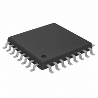
MAX3693ECJ Maxim Integrated Products, MAX3693ECJ Datasheet - Page 6

MAX3693ECJ
Manufacturer Part Number
MAX3693ECJ
Description
IC SERIALIZR 622MBPS LVDS 32TQFP
Manufacturer
Maxim Integrated Products
Datasheet
1.MAX3693ECJ.pdf
(8 pages)
Specifications of MAX3693ECJ
Function
Serializer
Data Rate
622Mbps
Input Type
LVDS
Output Type
PECL
Number Of Inputs
4
Number Of Outputs
1
Voltage - Supply
3 V ~ 3.6 V
Operating Temperature
-40°C ~ 85°C
Mounting Type
Surface Mount
Package / Case
32-LQFP
Lead Free Status / RoHS Status
Contains lead / RoHS non-compliant
Available stocks
Company
Part Number
Manufacturer
Quantity
Price
Part Number:
MAX3693ECJ
Manufacturer:
MAXIM/美信
Quantity:
20 000
Company:
Part Number:
MAX3693ECJ+
Manufacturer:
AKM
Quantity:
137
Company:
Part Number:
MAX3693ECJ+
Manufacturer:
Maxim Integrated
Quantity:
10 000
Company:
Part Number:
MAX3693ECJ+T
Manufacturer:
Maxim Integrated
Quantity:
10 000
The MAX3693 features LVDS inputs and outputs for
interfacing with high-speed digital circuitry. The LVDS
standard is based on the IEEE 1596.3 LVDS specifi-
cation. This technology uses 250mV to 400mV differ-
ential low-voltage swings to achieve fast transition
times, minimized power dissipation, and noise immu-
nity.
For proper operation, the parallel-clock LVDS outputs
(PCLKO+, PCLKO-) require 100Ω differential DC termi-
+3.3V, 622Mbps, SDH/SONET 4:1 Serializer
with Clock Synthesis and LVDS Inputs
Figure 2. Timing Diagram
6
_______________________________________________________________________________________
Low-Voltage Differential-Signal (LVDS)
PCLKO
PCLKI
PD_
SD
NOTE: SIGNALS SHOWN ARE DIFFERENTIAL. FOR EXAMPLE, PCLKO = (PCLKO+) - (PCLKO-).
*PD3 = D3; PD2 = D2; PD1 = D1; PD0 = D0.
VALID PARALLEL DATA*
Inputs and Outputs
t
SU
t
SKEW
t
H
nation between the inverting and noninverting outputs.
Do not terminate these outputs to ground.
The parallel data and parallel clock LVDS inputs (PD_+,
PD_-, PCLKI+, PCLKI-, RCLK+, RCLK-) are internally
terminated with 100Ω differential input resistance, and
therefore do not require external termination.
The serial-data PECL outputs (SD+, SD-) require 50Ω
DC termination to (V
Output Termination section).
D3
CC
D2
- 2V) (see the Alternative PECL-
D1
D0
PECL Outputs


