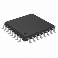
MAX3693ECJ Maxim Integrated Products, MAX3693ECJ Datasheet - Page 2

MAX3693ECJ
Manufacturer Part Number
MAX3693ECJ
Description
IC SERIALIZR 622MBPS LVDS 32TQFP
Manufacturer
Maxim Integrated Products
Datasheet
1.MAX3693ECJ.pdf
(8 pages)
Specifications of MAX3693ECJ
Function
Serializer
Data Rate
622Mbps
Input Type
LVDS
Output Type
PECL
Number Of Inputs
4
Number Of Outputs
1
Voltage - Supply
3 V ~ 3.6 V
Operating Temperature
-40°C ~ 85°C
Mounting Type
Surface Mount
Package / Case
32-LQFP
Lead Free Status / RoHS Status
Contains lead / RoHS non-compliant
Available stocks
Company
Part Number
Manufacturer
Quantity
Price
Part Number:
MAX3693ECJ
Manufacturer:
MAXIM/美信
Quantity:
20 000
Company:
Part Number:
MAX3693ECJ+
Manufacturer:
AKM
Quantity:
137
Company:
Part Number:
MAX3693ECJ+
Manufacturer:
Maxim Integrated
Quantity:
10 000
Company:
Part Number:
MAX3693ECJ+T
Manufacturer:
Maxim Integrated
Quantity:
10 000
ABSOLUTE MAXIMUM RATINGS
Terminal Voltage (with respect to GND)
Output Current
+3.3V, 622Mbps, SDH/SONET 4:1 Serializer
with Clock Synthesis and LVDS Inputs
DC ELECTRICAL CHARACTERISTICS
(V
wise noted. Typical values are at V
Stresses beyond those listed under “Absolute Maximum Ratings” may cause permanent damage to the device. These are stress ratings only, and functional
operation of the device at these or any other conditions beyond those indicated in the operational sections of the specifications is not implied. Exposure to
absolute maximum rating conditions for extended periods may affect device reliability.
2
PECL OUTPUTS (SD±)
LVDS INPUTS AND OUTPUTS (PCLKI±, RCLK±, PCLKO±, PD_±)
PROGRAMMING INPUT (CKSET)
Supply Current
Output High Voltage
Output Low Voltage
Input Voltage Range
Differential Input Threshold
Threshold Hysteresis
Differential Input Resistance
Output High Voltage
Output Low Voltage
Differential Output Voltage
Change in Magnitude of Differential Output
Voltage for Complementary States
Output Offset Voltage
Change in Magnitude of Output Offset Voltage
for Complementary States
Single-Ended Output Resistance
Change in Magnitude of Single-Ended Output
Resistance for Complementary Outputs
CKSET Input Current
CC
V
All Inputs, FIL+, FIL-,
LVDS Outputs (PCLKO±)................................................10mA
PECL Outputs (SD±).......................................................50mA
CC
_______________________________________________________________________________________
PCLKO+, PCLKO- ..............................-0.5V to (V
= +3V to +3.6V, differential LVDS loads = 100Ω ±1%, PECL loads = 50Ω ±1% to (V
.......................................................................-0.5V to +5V
PARAMETER
CC
= +3.3V, T
A
= +25°C.)
SYMBOL
CC
I
∆|V
V
V
∆V
CKSET
|V
∆R
V
V
V
V
V
HYST
R
I
IDTH
R
V
CC
OH
OH
OD
OL
OL
OS
IN
OD
+ 0.5V)
OS
O
I
O
|
|
PECL outputs unterminated
T
T
T
T
Differential input voltage =
100mV
Common-mode voltage =
50mV
CKSET = 0 or V
A
A
A
A
= 0°C to +85°C
= -40°C
= 0°C to +85°C
= -40°C
Continuous Power Dissipation (T
Operating Temperature Range ...........................-40°C to +85°C
Storage Temperature Range .............................-60°C to +160°C
Lead Temperature (soldering, 10s) .................................+300°C
CONDITIONS
TQFP (derate 10.20mW/°C above +85°C) ...................663mW
CC
CC
- 2V), T
V
V
V
V
0.925
1.125
CC
CC
CC
CC
-100
MIN
250
38
85
40
0
- 1.085
- 1.025
- 1.81
-1.83
A
= -40°C to +85°C, unless other-
A
±2.5
TYP
= +85°C)
100
65
60
95
V
V
V
V
CC
CC
CC
CC
1.475
1.275
- 1.555
MAX
±500
- 0.88
- 0.88
- 1.62
±25
±25
±10
100
100
115
400
140
2.4
UNITS
mA
mV
mV
mV
mV
mV
µA
%
Ω
Ω
V
V
V
V
V
V


