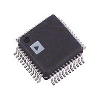
AD9846AJSTRL Analog Devices Inc, AD9846AJSTRL Datasheet - Page 9

AD9846AJSTRL
Manufacturer Part Number
AD9846AJSTRL
Description
IC CCD SIGNAL PROC 10BIT 48-LQFP
Manufacturer
Analog Devices Inc
Type
CCD Signal Processor, 10-Bitr
Datasheet
1.AD9846AJSTZRL.pdf
(24 pages)
Specifications of AD9846AJSTRL
Rohs Status
RoHS non-compliant
Input Type
Logic
Output Type
Logic
Interface
3-Wire Serial
Mounting Type
Surface Mount
Package / Case
48-LQFP
Analog Front End Type
CCD
Analog Front End Category
Video
Interface Type
Serial (3-Wire)
Sample Rate
30MSPS
Input Voltage Range
0.5V
Operating Supply Voltage (min)
2.7V
Operating Supply Voltage (typ)
3V
Operating Supply Voltage (max)
3.6V
Resolution
10b
Number Of Adc's
1
Power Supply Type
Analog/Digital
Operating Temp Range
-20C to 85C
Operating Temperature Classification
Commercial
Mounting
Surface Mount
Pin Count
48
Package Type
LQFP
Number Of Channels
1
Current - Supply
-
Lead Free Status / RoHS Status
Not Compliant
Available stocks
Company
Part Number
Manufacturer
Quantity
Price
CCD-MODE AND AUX MODE TIMING
OUTPUT
SIGNAL
CLPOB
CLPDM
DATACLK
DATA
PBLK
DATACLK
OUTPUT
CCD
SIGNAL
OUTPUT
SIGNAL
DATA
VIDEO
CCD
DATA
SHP
SHD
NOTES:
1. CLPOB AND CLPDM WILL OVERWRITE PBLK. PBLK WILL NOT AFFECT CLAMP OPERATION IF OVERLAPPING CLPDM AND/OR CLPOB.
2. PBLK SIGNAL IS OPTIONAL.
3. DIGITAL OUTPUT DATA WILL BE ALL ZEROS DURING PBLK. OUTPUT DATA LATENCY IS 9 DATACLK CYCLES.
NOTES:
1. RECOMMENDED PLACEMENT FOR DATACLK RISING EDGE IS BETWEEN THE SHD RISING EDGE AND NEXT SHP FALLING EDGE.
2. CCD SIGNAL IS SAMPLED AT SHP AND SHD RISING EDGES.
EFFECTIVE PIXELS
EFFECTIVE PIXEL DATA
t
ID
t
S1
N–10
N–10
t
INH
t
OD
t
OD
N
N
t
ID
t
ID
OPTICAL BLACK PIXELS
N–9
t
S2
N–9
N+1
OB PIXEL DATA
N+1
t
H
t
H
t
CP
t
N–8
CP
N–8
N+2
N+2
HORIZONTAL
BLANKING
N+8
DUMMY PIXELS
DUMMY BLACK
N–1
N–1
N+9
N+9
EFFECTIVE PIXELS
EFFECTIVE DATA
AD9846A
N
N
N+10
N+10


