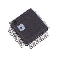
AD9846AJSTRL Analog Devices Inc, AD9846AJSTRL Datasheet - Page 19

AD9846AJSTRL
Manufacturer Part Number
AD9846AJSTRL
Description
IC CCD SIGNAL PROC 10BIT 48-LQFP
Manufacturer
Analog Devices Inc
Type
CCD Signal Processor, 10-Bitr
Datasheet
1.AD9846AJSTZRL.pdf
(24 pages)
Specifications of AD9846AJSTRL
Rohs Status
RoHS non-compliant
Input Type
Logic
Output Type
Logic
Interface
3-Wire Serial
Mounting Type
Surface Mount
Package / Case
48-LQFP
Analog Front End Type
CCD
Analog Front End Category
Video
Interface Type
Serial (3-Wire)
Sample Rate
30MSPS
Input Voltage Range
0.5V
Operating Supply Voltage (min)
2.7V
Operating Supply Voltage (typ)
3V
Operating Supply Voltage (max)
3.6V
Resolution
10b
Number Of Adc's
1
Power Supply Type
Analog/Digital
Operating Temp Range
-20C to 85C
Operating Temperature Classification
Commercial
Mounting
Surface Mount
Pin Count
48
Package Type
LQFP
Number Of Channels
1
Current - Supply
-
Lead Free Status / RoHS Status
Not Compliant
Available stocks
Company
Part Number
Manufacturer
Quantity
Price
D10
X
A/D Converter
The AD9846A uses high-performance ADC architecture, opti-
mized for high speed and low power. Differential Nonlinearity
(DNL) performance is typically better than 0.5 LSB, as shown in
TPC 2. Instead of the 1 V full-scale range used by the earlier
AD9801 and AD9803 products from Analog Devices, the
AD9846A ADC uses a 2 V input range. Better noise performance
results from using a larger ADC full-scale range (see TPC 3).
AUX1 Mode
For applications that do not require CDS, the AD9846A can be
configured to sample ac-coupled waveforms. Figure 30 shows
the circuit configuration for using the AUX1 channel input
(Pin 36). A single 0.1 µF ac-coupling capacitor is needed between
the input signal driver and the AUX1IN pin. An on-chip dc-bias
circuit sets the average value of the input signal to approximately
0.4 V, which is referenced to the midscale code of the ADC.
The VGA Gain register provides a gain range of 0 dB to 36 dB in
this mode of operation (see VGA Gain Curve, Figure 29).
The VGA gains up the signal level with respect to the 0.4 V bias
MSB
D9
0
1
1
0.8V
INPUT SIGNAL
SIGNAL
D8
X
0
1
VIDEO
0.4V
0.1 F
D7
X
0
1
0.1 F
??V
AUX2IN
Table VII. VGA Gain Register Used for AUX2-Mode
AUX1IN
D6
X
0
1
BUFFER
VIDEO CLAMP
0.4V
0.4V
CIRCUIT
5k
LPF
D5
X
0
•
•
•
1
VGA GAIN
REGISTER
VGA
9
D4
X
0
1
0dB TO 36dB
VGA GAIN
REGISTER
0dB TO 18dB
VGA
level. Signal levels above the bias level will be further increased
to a higher ADC code, while signal levels below the bias level
will be further decreased to a lower ADC code.
AUX2 Mode
For sampling video-type waveforms, such as NTSC and PAL
signals, the AUX2 channel provides black level clamping, gain
adjustment, and A/D conversion. Figure 31 shows the circuit
configuration for using the AUX2 channel input (Pin 34). A
external 0.1 µF blocking capacitor is used with the on-chip video
clamp circuit, to level-shift the input signal to a desired refer-
ence level. The clamp circuit automatically senses the most
negative portion of the input signal, and adjusts the voltage
across the input capacitor. This forces the black level of the
input signal to be equal to the value programmed into the Clamp
Level register (see Serial Interface Register Description). The VGA
provides gain adjustment from 0 dB to 18 dB. The same VGA
Gain register is used, but only the 9 MSBs of the gain register
are used (see Table VII.)
10
8
D3
X
0
1
CLAMP LEVEL
REGISTER
ADC
ADC
D2
X
0
1
D1
X
0
1
CLAMP LEVEL
LSB
D0
X
0
1
MIDSCALE
AD9846A
Gain (dB)
0.0
0.0
•
•
•
18.0


