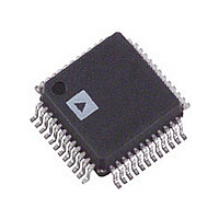
AD9846AJSTRL Analog Devices Inc, AD9846AJSTRL Datasheet - Page 14

AD9846AJSTRL
Manufacturer Part Number
AD9846AJSTRL
Description
IC CCD SIGNAL PROC 10BIT 48-LQFP
Manufacturer
Analog Devices Inc
Type
CCD Signal Processor, 10-Bitr
Datasheet
1.AD9846AJSTZRL.pdf
(24 pages)
Specifications of AD9846AJSTRL
Rohs Status
RoHS non-compliant
Input Type
Logic
Output Type
Logic
Interface
3-Wire Serial
Mounting Type
Surface Mount
Package / Case
48-LQFP
Analog Front End Type
CCD
Analog Front End Category
Video
Interface Type
Serial (3-Wire)
Sample Rate
30MSPS
Input Voltage Range
0.5V
Operating Supply Voltage (min)
2.7V
Operating Supply Voltage (typ)
3V
Operating Supply Voltage (max)
3.6V
Resolution
10b
Number Of Adc's
1
Power Supply Type
Analog/Digital
Operating Temp Range
-20C to 85C
Operating Temperature Classification
Commercial
Mounting
Surface Mount
Pin Count
48
Package Type
LQFP
Number Of Channels
1
Current - Supply
-
Lead Free Status / RoHS Status
Not Compliant
Available stocks
Company
Part Number
Manufacturer
Quantity
Price
SERIAL INTERFACE TIMING AND INTERNAL REGISTER DESCRIPTION
Register
Name
Operation
VGA Gain
Clamp Level
Control
PxGA Gain0
PxGA Gain1
PxGA Gain2
PxGA Gain3
AD9846A
Internal use only. Must be set to zero.
Must be set to one.
SDATA
SDATA
SCK
SCK
SL
SL
A0 A1 A2
0
1
0
1
0
1
0
1
NOTES:
1. RNW = READ-NOT WRITE. SET HIGH FOR READ OPERATION.
2. TEST BITS = INTERNAL USE ONLY. MUST BE SET LOW.
3. SERIAL DATA FROM THE SELECTED REGISTER IS VALID STARTING AFTER THE FIFTH SCK FALLING EDGE, AND IS UPDATED ON
NOTES:
1. SDATA BITS ARE INTERNALLY LATCHED ON THE RISING EDGES OF SCK.
2. RNW = READ-NOT WRITE. SET LOW FOR WRITE OPERATION.
3. TEST BITS = INTERNAL USE ONLY. MUST BE SET LOW.
4. SYSTEM UPDATE OF LOADED REGISTERS OCCURS ON SL RISING EDGE.
t
Address
t
DS
DS
SCK FALLING EDGES.
0
0
1
1
0
0
1
1
RNW
RNW
0
1
0
0
0
0
1
1
1
1
t
t
LS
LS
A0
A0
D0
Channel Select Power-Down
CCD/AUX1/2 Modes
LSB
LSB
Color Steering Mode
Selection
LSB
LSB
LSB
LSB
t
t
DH
DH
A1
A1
D1
A2
0
TEST BIT
TEST BIT
D2
0
0
Table I. Internal Register Map
D0
D0
t
Data Bits
PxGA
On/Off
DV
D3
D1
D1
D2
D4
Software OB Clamp
Reset
Clock Polarity Select for
SHP/SHD/CLP/DATA
D2
D3
D3
D5
On/Off
MSB
MSB
MSB
MSB
D4
D4
D5
D5
D6
D6
D6
0
X
X
X
X
D7
D7
D8
D8
1
0
D7
MSB
X
X
X
X
D9
D9
t
t
LH
LH
D10
D8
0
X
0
X
X
X
X
D10
D9
0
MSB
X
Three-
State
X
X
X
X
D10
0
X
X
X
X
X
X
X


