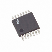
X96010V14IZ Intersil, X96010V14IZ Datasheet - Page 3

X96010V14IZ
Manufacturer Part Number
X96010V14IZ
Description
IC SENSOR CONDITIONER 14-TSSOP
Manufacturer
Intersil
Type
Sensor Conditionerr
Datasheet
1.X96010V14IZ.pdf
(26 pages)
Specifications of X96010V14IZ
Input Type
Voltage
Output Type
Voltage
Interface
2-Wire
Current - Supply
15mA
Mounting Type
Surface Mount
Package / Case
14-TSSOP
Lead Free Status / RoHS Status
Lead free / RoHS Compliant
Available stocks
Company
Part Number
Manufacturer
Quantity
Price
Company:
Part Number:
X96010V14IZ
Manufacturer:
IDT
Quantity:
989
ABSOLUTE MAXIMUM RATINGS
All voltages are referred to Vss.
Temperature under bias ................... -65°C to +100°C
Storage temperature ........................ -65°C to +150°C
Voltage on every pin except Vcc
Voltage on Vcc Pin .............................................0 to 5.5V
D.C. Output Current at pin SDA
D.C. Output Current at pins R1, R2, and
D.C. Output Current at pins I1 and I2 ....... -3.5 to +3.5mA
Lead temperature (soldering, 10s) .................... 300°C
RECOMMENDED OPERATING CONDITIONS
ELECTRICAL CHARACTERISTICS (Conditions are as follows, unless otherwise specified)
All typical values are for 25°C ambient temperature and 5V at pin Vcc. Maximum and minimum specifications are over
the recommended operating conditions. All voltages are referred to the voltage at pin Vss. Bit 3 in Control register 0 is
“1”, while all other bits in control registers are “0”. 255Ω, 0.1%, resistor connected between R1 and Vss, and another
between R2 and Vss. 400kHz TTL input at SCL. SDA pulled to Vcc through an external 2kΩ resistor. 2-wire interface
in “standby” (see notes 1 and 2 on page 5). WP, A0, A1, and A2 floating. VRef pin unloaded.
Temperature
Temperature while writing to memory
Voltage on Vcc Pin
Voltage on any other Pin
Iccstby
Iccfull
Iccwrite
I
V
V
I
V
I
V
PLDN
INTTL
OHSDA
VRef ........................................................ -0.50 to 1 mA
ILTTL
IHTTL
OLSDA
ILCMOS
Symbol
Standby current into Vcc
pin
Full operation current into
Vcc pin
Nonvolatile Write current
into Vcc pin
On-chip pull down current
at WP, A0, A1, and A2
SCL and SDA, input Low
voltage
SCL and SDA, input High
voltage
SCL and SDA input
current
SDA output Low voltage
SDA output High current
WP, A0, A1, and A2 input
Low voltage
Parameter
3
...................... 0 to 5 mA
................ -1.0V to +7V
Parameter
Min
2.0
-1
0
0
0
0
X96010
Typ
4
1
COMMENT
Stresses above those listed under “Absolute Maximum
Ratings” may cause permanent damage to the device.
This is a stress rating only; functional operation of the
device (at these or any other conditions above those
listed in the operational sections of this specification) is
not implied. Exposure to absolute maximum rating con-
ditions for extended periods may affect device reliability.
0.2 x
Max
100
Vcc
0.8
0.4
15
20
10
2
Unit
mA
mA
mA
µA
µA
µA
V
V
V
V
R1 and R2 floating, VRef unloaded.
2-wire interface reading from
memory, I
Vss, DAC input bytes: FFh, VRef
unloaded.
Average from START condition until
t
WP: Vcc, R1 and R2 floating,
VRef unloaded.
V(WP), V(A0), V(A1), and V(A2) from
0V to Vcc
Pin voltage between 0 and Vcc, and
SDA as an input.
I(SDA) = 2 mA
V(SDA) = Vcc
WP
after the STOP condition
Test Conditions / Notes
Min.
-0.3
-40
3
0
1
and I
2
Vcc + 0.3
both connected to
Max.
+100
+70
5.5
October 25, 2005
Units
°C
°C
FN8214.1
V
V


