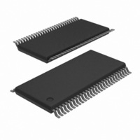
PCA9698DGG,518 NXP Semiconductors, PCA9698DGG,518 Datasheet - Page 29

PCA9698DGG,518
Manufacturer Part Number
PCA9698DGG,518
Description
IC I/O EXPANDER I2C 40B 56TSSOP
Manufacturer
NXP Semiconductors
Datasheet
1.PCA9698BS118.pdf
(48 pages)
Specifications of PCA9698DGG,518
Package / Case
56-TSSOP
Interface
I²C
Number Of I /o
40
Interrupt Output
Yes
Frequency - Clock
1MHz
Voltage - Supply
2.3 V ~ 5.5 V
Operating Temperature
-40°C ~ 85°C
Mounting Type
Surface Mount
Includes
POR
Logic Family
PCA9698
Number Of Lines (input / Output)
40.0 / 40.0
Operating Supply Voltage
2.3 V to 5.5 V
Power Dissipation
500 mW
Operating Temperature Range
- 40 C to + 85 C
Input Voltage
5.5 V
Logic Type
I2C Bus
Maximum Clock Frequency
1 MHz
Mounting Style
SMD/SMT
Number Of Input Lines
40.0
Number Of Output Lines
40.0
Output Current
50 mA
Output Voltage
5.5 V
Lead Free Status / RoHS Status
Lead free / RoHS Compliant
For Use With
OM6281 - DAUGHTER CARD PCA9698 FOR OM6275
Lead Free Status / Rohs Status
Lead free / RoHS Compliant
Other names
935278614518
PCA9698DGG-T
PCA9698DGG-T
PCA9698DGG-T
PCA9698DGG-T
NXP Semiconductors
PCA9698
Product data sheet
Fig 20. Read from output structure configuration, all bank control or mode selection registers
Fig 21. SMBus Alert procedure
Fig 22. Device ID field reading
SDA
SMBALERT
S A6 A5 A4 A3 A2 A1 A0 0 A
START condition
If AI = 0 or 1, the same register is read during the all sequence.
If more than 3 bytes are read, the slave device loops back to the first byte (manufacturer byte) and keeps sending data until the
master generates a ‘No Acknowledge’.
00 for output structure configuration register reading
01 for for all bank control register reading
10 for mode selection register reading
slave address
S 1
START condition
11
M
Device ID address
10 M9 M8 M7 M6 M5 M4
M
1
1
acknowledge
manufacturer name = 000000000000
one or several slaves
1
from slave
acknowledge from
1
R/W
0
slave receiver becomes slave-transmitter.
0
AI = 'don't care'
X
R/W
S 0
START condition
0 A
0
At this moment master-transmitter
command register
A M3 M2 M1 M0
acknowledge
from master
of the device to be identified
1
All information provided in this document is subject to legal disclaimers.
A6 A5 A4 A3 A2 A1 A0
becomes master-receiver and
response address
0
I
2
SMBus Alert
0
C-bus slave address
0
1
1
40-bit Fm+ I
Rev. 3 — 3 August 2010
acknowledge
0 D1 D0
1
from slave
0
P8 P7 P6 P5 A
don't care
part identification = 000000000
0
A
R/W
1 A
Sr
repeated START
condition
acknowledge from slave
that generated the alert
0 A
2
A6 A5 A4 A3 A2 A1 A0
C-bus advanced I/O port with RESET, OE and INT
A6 A5 A4 A3 A2 A1 A0 0
acknowledge from
slave to be identified
Sr
acknowledge
from master
PCA9698 I
repeated START
condition
slave address
slave address
P4 P3 P2 P1 P0 R2 R1 R0
1
Device ID address
1
2
1
C-bus
acknowledge
1
from slave
1
revision = 000
R/W
1 A
R/W
0
At this moment master-transmitter
becomes master-receiver, and
slave-receiver becomes slave-transmitter.
A
no acknowledge
from master
0
R/W
P
STOP condition
1 A
data from register
SMBALERT signal is released
(assuming that only one device
generated the alert)
A
no acknowledge
from master
acknowledge from
slave to be identified
last byte
P
STOP condition
DATA
no acknowledge
PCA9698
002aab951
from master
© NXP B.V. 2010. All rights reserved.
condition
STOP
002aab950
A
P
002aab949
29 of 48


