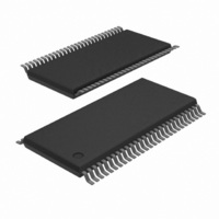
PCA9698DGG,518 NXP Semiconductors, PCA9698DGG,518 Datasheet - Page 20

PCA9698DGG,518
Manufacturer Part Number
PCA9698DGG,518
Description
IC I/O EXPANDER I2C 40B 56TSSOP
Manufacturer
NXP Semiconductors
Datasheet
1.PCA9698BS118.pdf
(48 pages)
Specifications of PCA9698DGG,518
Package / Case
56-TSSOP
Interface
I²C
Number Of I /o
40
Interrupt Output
Yes
Frequency - Clock
1MHz
Voltage - Supply
2.3 V ~ 5.5 V
Operating Temperature
-40°C ~ 85°C
Mounting Type
Surface Mount
Includes
POR
Logic Family
PCA9698
Number Of Lines (input / Output)
40.0 / 40.0
Operating Supply Voltage
2.3 V to 5.5 V
Power Dissipation
500 mW
Operating Temperature Range
- 40 C to + 85 C
Input Voltage
5.5 V
Logic Type
I2C Bus
Maximum Clock Frequency
1 MHz
Mounting Style
SMD/SMT
Number Of Input Lines
40.0
Number Of Output Lines
40.0
Output Current
50 mA
Output Voltage
5.5 V
Lead Free Status / RoHS Status
Lead free / RoHS Compliant
For Use With
OM6281 - DAUGHTER CARD PCA9698 FOR OM6275
Lead Free Status / Rohs Status
Lead free / RoHS Compliant
Other names
935278614518
PCA9698DGG-T
PCA9698DGG-T
PCA9698DGG-T
PCA9698DGG-T
NXP Semiconductors
PCA9698
Product data sheet
7.12 Output enable input (OE)
7.13 Live insertion
7.14 Standby
The configurable active LOW or active HIGH output enable pin allows to enable or disable
all the I/Os at the same time.
For applications requiring LED blinking with brightness control, this pin can be used to
control the brightness by applying a high frequency PWM signal on the OE pin. LEDs can
be blinked using the Output Port registers and can be dimmed using the PWM signal on
the OE pin thus controlling the brightness by adjusting the duty cycle.
Default is OEPOL = 0, so if the OE pin is held HIGH, the outputs are disabled. The OE pin
needs to be pulled LOW or OEPOL changed to ‘1’ to enable the outputs.
It is recommended to define the required polarity of the OE input by programing the value
of OEPOL before programming the configuration registers (IOC register).
The PCA9698 is fully specified for live-insertion applications using I
3-states, robust state machine, and 50 ns noise filter. The I
outputs, preventing damaging current backflow through the device when it is powered
down. The power-up 3-states circuitry places the outputs in the high-impedance state
during power-up and power-down, which prevents driver conflict and bus contention.
The robust state machine does not respond until it sees a valid START condition and the
50 ns noise filter will filter out any insertion glitches. The PCA9698 will not cause
corruption of active data on the bus nor will the device be damaged or cause damage to
devices already on the bus when similar featured devices are being used.
The PCA9698 goes into standby when the I
than 1.0 μA (typical).
•
•
When a LOW level is applied to the OE pin, with OEPOL = 0 (register 2Ah, bit 4) or a
HIGH level is applied to the OE pin, with OEPOL = 1 (register 2Ah, bit 0), all the I/Os
configured as outputs are enabled and the logic value programmed in their respective
OP registers is applied to the pins.
When a HIGH level is applied to the OE pin, with OEPOL = 0 (register 2Ah, bit 0) or a
LOW level is applied to the OE pin, with OEPOL = 1 (register 2Ah, bit 0), all the I/Os
configured as outputs are 3-stated.
All information provided in this document is subject to legal disclaimers.
40-bit Fm+ I
Rev. 3 — 3 August 2010
2
C-bus advanced I/O port with RESET, OE and INT
2
C-bus is idle. Standby supply current is lower
OFF
circuitry disables the
OFF
PCA9698
, power-up
© NXP B.V. 2010. All rights reserved.
20 of 48


