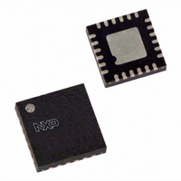
PCA9502BS,128 NXP Semiconductors, PCA9502BS,128 Datasheet - Page 6

PCA9502BS,128
Manufacturer Part Number
PCA9502BS,128
Description
IC I/O EXPANDER I2C/SPI 24HVQFN
Manufacturer
NXP Semiconductors
Datasheet
1.PCA9502BS157.pdf
(25 pages)
Specifications of PCA9502BS,128
Package / Case
24-VQFN Exposed Pad, 24-HVQFN, 24-SQFN, 24-DHVQFN
Interface
I²C, SPI
Number Of I /o
8
Interrupt Output
No
Frequency - Clock
400kHz
Voltage - Supply
2.3 V ~ 3.6 V
Operating Temperature
-40°C ~ 85°C
Mounting Type
Surface Mount
Logic Family
PCA9502
Number Of Lines (input / Output)
8.0 / 8.0
Operating Supply Voltage
2.5 V to 3.3 V
Power Dissipation
300 mW
Operating Temperature Range
- 40 C to + 85 C
Input Voltage
5.5 V
Logic Type
I/O Expander
Maximum Clock Frequency
400 KHz
Mounting Style
SMD/SMT
Number Of Input Lines
8.0
Number Of Output Lines
8.0
Output Current
10 mA
Output Voltage
5.5 V
Lead Free Status / RoHS Status
Lead free / RoHS Compliant
Lead Free Status / RoHS Status
Lead free / RoHS Compliant, Lead free / RoHS Compliant
Other names
935281363128
PCA9502BS-F
PCA9502BS-F
PCA9502BS-F
PCA9502BS-F
NXP Semiconductors
PCA9502_3
Product data sheet
8.2 Programmable I/O pins State register (IOState)
8.3 I/O Interrupt Enable register (IOIntEna)
8.4 I/O Control register (IOControl)
When ‘read’, this register returns the actual state of all I/O pins. When ‘write’, each
register bit will be transferred to the corresponding IO pin programmed as output.
Table 8.
This register enables the interrupt due to a change in the I/O configured as inputs.
Table 9.
Table 10.
Bit
7:0
Bit
7:0
Bit
7:4
3
2:1
0
Symbol
IOState
Symbol
IOIntEna
Symbol
-
SReset
-
IOLatch
IOState register (address 0x0B) bit description
IOIntEna register (address 0x0C) bit description
IOControl register (address 0x0E) bit description
Rev. 03 — 13 October 2006
Description
Write this register: set the logic level on the output pins
Read this register: return states of all pins
Description
input interrupt enable
Description
reserved for future use
software reset
reserved for future use
enable/disable inputs latching
Example: If GPIO4 input was as logic 0 and the input goes to logic 1
then back to logic 0, the IOState register will capture this change and
an interrupt is generated (if enabled). When the read is performed on
the IOState register, the interrupt is de-asserted, assuming there were
no additional input(s) that changed, and bit 4 of the IOState register
will read ‘1’. The next read of the IOState register should now read ‘0’.
0 = a change in the input pin will not generate an interrupt
1 = a change in the input will generate an interrupt
A write to this bit will reset the device. Once the device is reset this
bit is automatically set to 0.
0 = input values are not latched. A change in any input generates an
interrupt. A read of the input register clears the interrupt. If the input
goes back to its initial logic state before the input register is read,
then the interrupt is cleared.
1 = input values are latched. A change in the input generates an
interrupt and the input logic value is loaded in the bit of the
corresponding input state register (IOState). A read of the IOState
register clears the interrupt. If the input pin goes back to its initial
logic state before the interrupt register is read, then the interrupt is
not cleared and the corresponding bit of the IOState register keeps
the logic value that initiates the interrupt.
0 = set output pin to zero
1 = set output pin to one
8-bit I/O expander with I
2
C-bus/SPI interface
PCA9502
© NXP B.V. 2006. All rights reserved.
6 of 25


