LTC6605CDJC-7#PBF Linear Technology, LTC6605CDJC-7#PBF Datasheet - Page 5

LTC6605CDJC-7#PBF
Manufacturer Part Number
LTC6605CDJC-7#PBF
Description
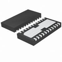
IC FILTER 7MHZ DUAL 22-DFN
Manufacturer
Linear Technology
Datasheet
1.LTC6605CDJC-7PBF.pdf
(20 pages)
Specifications of LTC6605CDJC-7#PBF
Filter Type
Antialiasing
Frequency - Cutoff Or Center
5MHz
Number Of Filters
2
Max-order
2nd
Voltage - Supply
2.7 V ~ 5.25 V
Mounting Type
Surface Mount
Package / Case
22-DFN
No. Of Amplifiers
2
Input Offset Voltage
1mV
Gain Db Max
14dB
Bandwidth
7MHz
Supply Voltage Range
2.7V To 5.25V
Supply Current
33.1mA
Amplifier Case Style
DFN
No. Of Pins
22
Rohs Compliant
Yes
Lead Free Status / RoHS Status
Lead free / RoHS Compliant
Available stocks
Company
Part Number
Manufacturer
Quantity
Price
ELECTRICAL CHARACTERISTICS
Note 8: See the Applications Information section for a detailed
discussion of input and output common mode range. Input common
mode range is tested by measuring the differential DC gain with V
= mid-supply, and again with V
limits listed in the Electrical Characteristics table, with ΔV
verifying that the differential gain has not deviated from the mid-supply
common mode input case by more than 0.5%, and that the common
mode offset (V
mode offset by more than ±10mV.
Output common mode range is tested by measuring the differential
DC gain with V
V
TYPICAL PERFORMANCE CHARACTERISTICS
OCM
pin at the output common range limits listed in the Electrical
OSCM
OCM
= mid-supply, and again with voltage set on the
–0.5
–1.5
) has not deviated from the mid-supply common
30.0
15.0
12.5
–1.0
37.5
35.0
32.5
27.5
25.0
22.5
20.0
17.5
1.0
0.5
0
–60
–60
Supply Current vs Temperature
–3dB Frequency vs Temperature
V
INCM
–40
–40
BIAS = FLOAT
BIAS = V
INCM
= V
–20
–20
OCM
TEMPERATURE (°C)
at the input common mode range
TEMPERATURE (°C)
+
= MID-SUPPLY
0
0
V
V
V
V
V
V
20
20
S
S
S
S
S
S
= 2.7V, BIAS = FLOAT
= 3V, BIAS = FLOAT
= 5V, BIAS = FLOAT
= 2.7V, BIAS = V
= 3V, BIAS = V
= 5V, BIAS = V
V
V
S
INCM
= 3V
40
40
= V
60
60
OCM
+
+
= 1.5V
80
80
IN
66057 G03
+
66057 G01
= ±0.25V,
100
100
INCM
Characteristics table, verifying that the differential gain has not
deviated from the mid-supply common mode input case by more than
0.5%, and that the common mode offset (V
more than ±10mV from the mid-supply case.
Note 9: CMRR is defi ned as the ratio of the change in the input common
mode voltage at the internal amplifi er inputs to the change in differential
input referred voltage offset (V
Note 10: Power supply rejection ratio (PSRR) is defi ned as the ratio of
the change in supply voltage to the change in differential input referred
voltage offset (V
1.010
1.005
1.000
0.990
0.995
–10
–20
–30
–40
–50
–60
10
0
0.1
–60
Filter Gain vs Temperature
Filter Frequency Response
V
V
5 REPRESENTATIVE UNITS
S
INCM
–40
= 3V, BIAS = V
BIAS = V
BIAS PIN FLOATING
OS
= V
–20
).
1
OCM
TEMPERATURE (°C)
FREQUENCY (MHz)
+
= MID-SUPPLY
0
+
10
20
OS
40
).
100
60
80
66057 G04
66057 G02
OSCM
LTC6605-7
1000
100
) has not deviated by
66057f
5


