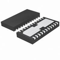
LTC6605CDJC-7#PBF Linear Technology, LTC6605CDJC-7#PBF Datasheet - Page 15

LTC6605CDJC-7#PBF
Manufacturer Part Number
LTC6605CDJC-7#PBF
Description
IC FILTER 7MHZ DUAL 22-DFN
Manufacturer
Linear Technology
Datasheet
1.LTC6605CDJC-7PBF.pdf
(20 pages)
Specifications of LTC6605CDJC-7#PBF
Filter Type
Antialiasing
Frequency - Cutoff Or Center
5MHz
Number Of Filters
2
Max-order
2nd
Voltage - Supply
2.7 V ~ 5.25 V
Mounting Type
Surface Mount
Package / Case
22-DFN
No. Of Amplifiers
2
Input Offset Voltage
1mV
Gain Db Max
14dB
Bandwidth
7MHz
Supply Voltage Range
2.7V To 5.25V
Supply Current
33.1mA
Amplifier Case Style
DFN
No. Of Pins
22
Rohs Compliant
Yes
Lead Free Status / RoHS Status
Lead free / RoHS Compliant
Available stocks
Company
Part Number
Manufacturer
Quantity
Price
APPLICATIONS INFORMATION
Noise
When comparing the LTC6605-7’s noise to that of other
amplifi ers, be sure to compare similar specifi cations. Stand-
alone op amps often specify noise referred to the inputs of the
op amp. The LTC6605-7’s internal op amp has input referred
voltage noise of only 2.1nV/√Hz. In addition to the noise gen-
erated by the amplifi er, the surrounding feedback resistors
also contribute noise. A noise model is shown in Figure 7a.
The output spot noise generated by both the amplifi er
and the feedback components is given in Figure 7b.
e
e
no
no
=
=
e
e
ni
ni
• 1+
• 1+
R2
R1
R2
R1
2
2
+ 2 • I
+ 2 • I
n
n
• R2 + R3 • 1+
• R2 + R3 • 1+
e
e
nR1
nR1
2
2
R1
R1
Figure 7a. Differential Noise Model
R2
e
e
R2
R1
R1
nR3
nR3
2
2
I
I
n
n
Figure 7b
2
Figure 7c
R3
R3
2
+ 2
– 2
+ 2 • e
+ 8 • k • T • R2 • 1+
Substituting the equation for Johnson noise of a resistor
(e
ing gives the result shown in Figure 7c.
Board Layout and Bypass Capacitors
For single-supply applications it is recommended that a
high quality X5R or X7R, 0.1μF bypass capacitor be placed
directly between V
including the Exposed Pad, should be tied directly to a low
impedance ground plane with minimal routing.
e
ni
e
e
nR2 2
2
nR2
2
nR1
nR
2
+
–
= 4kTR) into the equation in Figure 7b and simplify-
•
R2
R2
R2
R1
66057 F07a
2
+ 2 • e
R2
e
R1
no
+
2
and the adjacent V
+ R3 • 1+
nR3
• 1+
R2
R1
R2
R1
LTC6605-7
2
2
+ 2 • e
–
pin. The V
nR2
2
15
–
pins,
66057f


