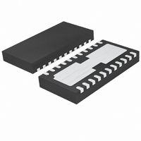
LTC6605CDJC-7#PBF Linear Technology, LTC6605CDJC-7#PBF Datasheet - Page 3

LTC6605CDJC-7#PBF
Manufacturer Part Number
LTC6605CDJC-7#PBF
Description
IC FILTER 7MHZ DUAL 22-DFN
Manufacturer
Linear Technology
Datasheet
1.LTC6605CDJC-7PBF.pdf
(20 pages)
Specifications of LTC6605CDJC-7#PBF
Filter Type
Antialiasing
Frequency - Cutoff Or Center
5MHz
Number Of Filters
2
Max-order
2nd
Voltage - Supply
2.7 V ~ 5.25 V
Mounting Type
Surface Mount
Package / Case
22-DFN
No. Of Amplifiers
2
Input Offset Voltage
1mV
Gain Db Max
14dB
Bandwidth
7MHz
Supply Voltage Range
2.7V To 5.25V
Supply Current
33.1mA
Amplifier Case Style
DFN
No. Of Pins
22
Rohs Compliant
Yes
Lead Free Status / RoHS Status
Lead free / RoHS Compliant
Available stocks
Company
Part Number
Manufacturer
Quantity
Price
DC ELECTRICAL CHARACTERISTICS
SYMBOL
V
CMRR
PSRR
V
V
V
R
V
I
V
I
R
t
t
temperature range, otherwise specifi cations are at T
R
V
SC
S
ON
OFF
INCM
OSCM
OCM
MID
OUT
S
VOCM
BIAS
–OUT
BAL
= 10k. The fi lter is confi gured for a gain of 1, unless otherwise noted. V
)/2. V
INCM
is defi ned as (V
PARAMETER
Input Common Mode Voltage Range
(Note 8)
Common Mode Rejection Ratio
(ΔV
Power Supply Rejection Ratio
(ΔV
Common Mode Offset Voltage
(V
Output Common Mode Range
(Valid Range for V
Self-Biased Voltage at the V
Input Resistance of V
Output Voltage Swing, High
(Measured Relative to V
Output Voltage Swing, Low
(Measured Relative to V
Output Short-Circuit Current (Note 3)
Supply Voltage
Supply Current (per Channel)
BIAS Pin Range for Shutdown
BIAS Pin Range for Medium Power
BIAS Pin Range for Full Power
BIAS Pin Self-Biased Voltage (Floating) Referenced to V
BIAS Pin Input Resistance
Turn-On Time
Turn-Off Time
OUTCM
INCM
S
/ΔV
/ΔV
OS
– V
) (Note 10)
OS
OCM
) (Note 9)
INP
)
OCM
+ V
OCM
INM
Pin) (Note 8)
+
–
)
)
)/2. V
Pin
OCM
OUTDIFF
Pin
A
= 25°C. V
is defi ned as (V
CONDITIONS
V
V
V
V
V
V
V
V
V
V
V
V
V
V
V
V
V
V
V
V
V
V
V
V
V
V
V
Referenced to V
Referenced to V
Referenced to V
V
V
S
S
S
S
S
S
S
S
S
S
S
S
S
S
S
S
S
S
S
S
S
S
S
S
S
S
S
S
S
= 3V
= 5V
= 3V; ΔV
= 5V; ΔV
= 2.7V to 5V
= 3V
= 5V
= 3V
= 5V
= 3V
= 3V; I
= 3V; I
= 3V; I
= 5V; I
= 5V; I
= 5V; I
= 3V; I
= 3V; I
= 3V; I
= 5V; I
= 5V; I
= 5V; I
= 3V
= 5V
= 2.7V to 5V; BIAS = V
= 2.7V to 5V; BIAS = Floating
= 2.7V to 5V; BIAS = V
= 3V, V
= 3V, V
+
L
L
L
L
L
L
L
L
L
L
L
L
BIAS
BIAS
= 3V, V
The
= 0mA
= 5mA
= 20mA
= 0mA
= 5mA
= 20mA
= 0mA
= –5mA
= –20mA
= 0mA
= –5mA
= –20mA
INCM
INCM
= V
= V
l
–
–
–
–
+OUT
= 1.5V
= 2.5V
+
denotes the specifi cations which apply over the full operating
–
–
to V
to V
= 0V, V
– V
S
+
–
is defi ned as (V
+
–
–OUT
INCM
). V
= V
INDIFF
OCM
is defi ned as (V
= mid-supply, BIAS tied to V
+
l
l
l
l
l
l
l
l
l
l
l
l
l
l
l
l
l
l
l
l
l
l
l
l
l
l
l
l
l
l
l
l
l
l
– V
–
). V
1.475
–0.2
–0.2
MIN
12.5
1.05
±40
±50
100
2.7
2.3
1.1
1.1
46
46
66
0
1
OUTCM
INP
LTC6605-7
is defi ned as (V
33.1
16.2
0.35
TYP
1.15
245
285
415
350
390
550
120
135
195
175
200
270
±70
±95
150
400
400
±10
±10
1.5
95
74
74
18
– V
INM
). See Figure 1.
1.525
MAX
1000
23.5
5.25
26.5
1.25
450
525
750
625
700
225
250
350
325
360
475
200
±15
±15
4.7
1.6
0.4
1.5
1.7
45
V
2
4
+
S
, R
L
+OUT
= Open,
UNITS
66057f
3
+
mV
mV
mV
mV
mV
mV
mV
mV
mV
mV
mV
mV
mV
mV
mA
mA
mA
mA
mA
kΩ
kΩ
dB
dB
dB
ns
ns
V
V
V
V
V
V
V
V
V
V


