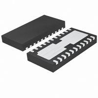
LTC6605CDJC-7#PBF Linear Technology, LTC6605CDJC-7#PBF Datasheet - Page 11

LTC6605CDJC-7#PBF
Manufacturer Part Number
LTC6605CDJC-7#PBF
Description
IC FILTER 7MHZ DUAL 22-DFN
Manufacturer
Linear Technology
Datasheet
1.LTC6605CDJC-7PBF.pdf
(20 pages)
Specifications of LTC6605CDJC-7#PBF
Filter Type
Antialiasing
Frequency - Cutoff Or Center
5MHz
Number Of Filters
2
Max-order
2nd
Voltage - Supply
2.7 V ~ 5.25 V
Mounting Type
Surface Mount
Package / Case
22-DFN
No. Of Amplifiers
2
Input Offset Voltage
1mV
Gain Db Max
14dB
Bandwidth
7MHz
Supply Voltage Range
2.7V To 5.25V
Supply Current
33.1mA
Amplifier Case Style
DFN
No. Of Pins
22
Rohs Compliant
Yes
Lead Free Status / RoHS Status
Lead free / RoHS Compliant
Available stocks
Company
Part Number
Manufacturer
Quantity
Price
APPLICATIONS INFORMATION
Setting the passband gain (GAIN = R2/R1) only requires
choosing a value for R1, since R2 is a fi xed internal 400Ω.
Therefore, the following three gains can be easily confi gured
without external components:
Table 1. Confi guring the Passband Gain Without External
Components
The resonant frequency, f
therefore independent of the gain. For any LTC6605-7 fi lter
confi guration that conforms to Figure 3, the f
7.98MHz. The f
tion of f
the selection of R4.
Setting the f
Using an external resistor (R
justable in the range of 6.5MHz to 10.0MHz (see Figure 3).
The minimum f
maximum f
gain less than 1dB.
Table 2. R
R1 = 400Ω, R4A = R4B = 100Ω
Figure 4 shows three filter configurations with an
f
–3dB
GAIN
(V/V)
f
–3dB
1
4
5
= 6.5MHz, without any external components. These
6.5
7.5
8.5
9.5
10
7
8
9
(MHz)
O
EXT
and Q. For any specifi c gain, Q is adjusted by
GAIN (dB)
–3dB
Selection GAIN = 1,
–3dB
12
14
0
–3dB
–3dB
is arbitrarily set for a maximum passband
Frequency
frequency depends on the combina-
is set for R
R
R1 (Ω)
12.7
24.9
39.2
54.9
73.2
95.3
EXT
124
400
100
80
0
Ω
O
EXT
, is independent of R1, and
Drive the 400Ω Resistors. Tie
the 100Ω Resistors Together.
Drive the 100Ω Resistors.
Drive the 400Ω and 100Ω
Resistors in Parallel.
), the f
EXT
INPUT PINS TO USE
equal to 0Ω and the
–3dB
frequency is ad-
O
is fi xed at
fi lters have a Q = 0.59, which is an almost ideal Bessel
characteristic with linear phase.
Figure 5 shows three fi lter confi gurations that use some
external resistors, and are tailored for a very fl at ±0.4dB
6.7MHz passband.
Many other confi gurations are possible by using the equa-
tions in Figure 3. For example, external resistors can be
added to modify the value of R1 to confi gure GAIN ≠ 1. For
an even more fl exible fi lter IC with similar performance,
consider the LTC6601.
BIAS Pin
Each channel of the LTC6605-7 has a BIAS pin whose
function is to tailor both performance and power. The BIAS
pin can be modeled as a voltage source whose potential
is 1.15V above the V
equivalent resistance of 150k. This three-state pin has fi xed
logic levels relative to V
table), and can be driven by any external source that can
drive the BIAS pin’s equivalent input impedance.
If the BIAS pin is tied to the positive supply, the part is
in a fully active state confi gured for highest performance
(lowest noise and lowest distortion).
If the BIAS pin is fl oated (left unconnected), the part is in
a fully active state, but with amplifi er currents reduced and
performance scaled back to preserve power consumption.
Care should be taken to limit external leakage currents
to this pin to under 1μA to avoid putting the part in an
unexpected state.
If the BIAS pin is tied to the most negative supply (V
the part is in a low power shutdown mode with amplifi er
outputs disabled. In shutdown, all internal biasing current
sources are shut off, and the output pins each appear as
open collectors with a non-linear capacitor in parallel and
steering diodes to either supply. Because of the non-linear
capacitance, the outputs can still sink and source small
amounts of transient current if exposed to signifi cant
voltage transients. Using this function to wire-OR outputs
together is not recommended.
–
–
supply and that has a Thevenin
(see the Electrical Characteristics
LTC6605-7
11
66057f
–
),


