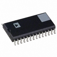
AD1892JR Analog Devices Inc, AD1892JR Datasheet - Page 6

AD1892JR
Manufacturer Part Number
AD1892JR
Description
IC SAMPLE CONV W/RX 20BIT 28SOIC
Manufacturer
Analog Devices Inc
Type
Sample Rate Converterr
Datasheet
1.AD1892JR.pdf
(24 pages)
Specifications of AD1892JR
Rohs Status
RoHS non-compliant
Applications
Players, Recorders
Voltage - Supply, Digital
4.5 V ~ 5.5 V
Mounting Type
Surface Mount
Package / Case
28-SOIC (7.5mm Width)
Voltage - Supply, Analog
-
Available stocks
Company
Part Number
Manufacturer
Quantity
Price
Part Number:
AD1892JRZ
Manufacturer:
ADI/亚德诺
Quantity:
20 000
AD1892
Subframe Status Outputs
Pin Name SOIC
NOSIG
ERROR
INT
U/CBIT
SFCLK
Q-Channel Subcode Clock Output Signal
Pin Name SOIC
QDFS
Serial Control Port Signals
Pin Name SOIC
CS
CCLK
SDI
SDO
12
11
10
9
8
6
3
2
4
5
I/O
O
O
O
O
O
I/O
O
I/O
I
I
I
O
Description
NOSIG (No Signal) is asserted HI when no biphase-mark input is applied to the AD1892 when
either the input sample rate is too high for the applied master clock (MCLK) frequency or, equiva-
lently, the master clock frequency is too low for the applied input sample rate. NOSIG is deasserted
LO during normal operation. This signal is asynchronous and has no particular timing relationship
with any of the clock signals associated with the AD1892.
The ERROR pin is asserted HI when either a subframe parity error or a subframe validity error
occurs. Logically, ERROR = PARITY ERROR or VALIDITY ERROR. The ERROR pin is deas-
serted LO when neither parity nor validity errors are detected. The state of this output pin is not
directly reflected in the AD1892 status registers; rather, Status Register 0 has separate bits that
indicate parity and validity errors. The ERROR output should be clocked using the SFCLK signal
(Pin 8). The ERROR output signal is NOT sticky, so it can be used in applications that do not in-
clude a supporting microcontroller.
INT (Interrupt) is asserted HI when any of the first 32 bits of Channel Status information changes
from block to block or when the Q-Channel subcode track number (Q10 through Q17) changes
from block to block (valid in consumer mode only). The Channel Status block spans 192 frames (or
subframes, since either the left or right channel C bit is stored), and the Q-Channel subcode block
spans 1176 subframes. INT is deasserted LO when neither the first 32 bits of Channel Status
changes from block to block when the Q-Channel subcode track number changes from block to
block. This output is mirrored in a status bit (Status Register 0, Bit 5). The INT output can be
clocked using the SFCLK signal (Pin 8). The INT output signal is sticky and can only be cleared by
reading Status Register 0.
U/CBIT is either the subframe user bit or the Channel Status bit from the biphase-mark stream, fed
out serially, valid on the rising edge of the SFCLK signal (Pin 8). The choice between user bit and
Channel Status bit is determined by Bit 1 in Control Register 0 (0 user bit [default], 1 = Channel
Status bit). Changes at the subframe rate (two times the incoming sample rate.) See Figure 39 for
timing.
This SFCLK signal is used to clock the ERROR, INT and U/CBIT output status signals. Active
LO (rising edge active); see Figure 39 for timing. It is a LO pulse at the subframe rate (two times
the sample rate). The pulsewidth is approximately 1/64th of the incoming sample (frame) period.
Description
QDFS (Q-Channel Data Frame Sync) is a framing pulse indicating if the AD1892 has finished col-
lecting a full Q-Channel subcode block of user bits, which has a period of 1176 subframes. Can be
used as an interrupt signal to a microcontroller. The QDFS output is HI for one subframe period.
The QDFS frequency is 75 Hz when the incoming input sample rate is 44.1 kHz. See Figure 40 for
timing information.
Description
Chip Select/Latch signal for the serial control port. This input must be LO for any write or read
operation using the serial control port to be valid. This input should be tied HI when using the
AD1892 in a stand-alone (no external microcontroller) application. See the Serial Control Port
Timing in Figure 37 and the text below for more information.
Serial Control Port Clock. This rising edge active input samples the address and data associated
with the serial control port. The frequency of CCLK signal must not exceed 1/8 the frequency of
the MCLK (Pin 28) signal. See the Serial Control Port Timing in Figure 37 and the text below for
more information.
Serial Data Input. This input signal is used to convey the serial 6-bit address, the read/write indication
and the 8-bit write data for the AD1892 serial control port. See the Serial Control Port Timing in
Figure 37 and the text below for more information.
Serial Data Output. This three-state output is used to convey the serial 8-bit read data for the
AD1892 serial control port. It is a three-state output to allow multiple AD1892s to coexist on the same
SPI serial bus. See the Serial Control Port Timing in Figure 37 and the text below for more information.
–6–
REV. 0


