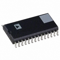
AD1892JR Analog Devices Inc, AD1892JR Datasheet - Page 13

AD1892JR
Manufacturer Part Number
AD1892JR
Description
IC SAMPLE CONV W/RX 20BIT 28SOIC
Manufacturer
Analog Devices Inc
Type
Sample Rate Converterr
Datasheet
1.AD1892JR.pdf
(24 pages)
Specifications of AD1892JR
Rohs Status
RoHS non-compliant
Applications
Players, Recorders
Voltage - Supply, Digital
4.5 V ~ 5.5 V
Mounting Type
Surface Mount
Package / Case
28-SOIC (7.5mm Width)
Voltage - Supply, Analog
-
Available stocks
Company
Part Number
Manufacturer
Quantity
Price
Part Number:
AD1892JRZ
Manufacturer:
ADI/亚德诺
Quantity:
20 000
REV. 0
SERIAL CONTROL PORT
The serial control port on the AD1892 is a bidirectional inter-
face that allows external microcontrollers and microprocessors
to gain access to the two on-chip byte-wide control registers and
to the sixteen on-chip byte-wide status registers. The serial
control port is signal compatible with the Serial Peripheral In-
terface (SPI) standard, which has been popularized by Motorola’s
family of microcontroller and microprocessor products.
The basic timing for the serial control port is shown in Figure
17. The CS signal is both a chip select and a latch enable. CS
must be LO for the duration of the read or write cycle. The
CCLK signal is the data clock signal for the serial control port.
The frequency of the CCLK signal must not exceed 1/8 the
frequency of the MCLK signal applied to the AD1892. The
incoming address and write data must be valid on the rising
edge of CCLK, and the outgoing read data is guaranteed to be
valid on the ring edge of CCLK. The SDI signal carries the
serial address and write data to the AD1892. The SDO signal
carries the serial read data from the AD1892. The address and
data information is MSB first.
CCLK
CCLK
SDO
SDO
SDI/SDO
SDI
SDI
CS
CS
CCLK
CS
ADDR5
MSB
ADDR5
MSB
ADDRESS
ADDRESS
ADDR4
ADDR4
Figure 17. Serial Control Port Basic Timing
Figure 18. Serial Control Port Write Cycle
Figure 19. Serial Control Port Read Cycle
MSB
MSB–1
ADDR0
ADDR0
LSB
LSB
HIGH Z
HIGH Z
MSB–2
R/W
R/W
–13–
RES
The serial control port write cycle is shown in Figure 18. In the
first byte, the AD1892 defines a six bit write address field, a
read/write bit (reset LO for a write cycle) and a reserved (res)
bit. [The reserve (res) bit should be reset LO for both write
and read cycles.] The data byte intended to be written to the
specified write address follows immediately thereafter, MSB
first. All information is carried on the SDI input, with the SDO
output remaining in a high impedance (three-state) condition.
The AD1892 defines only two valid write addresses, Control
Register 1 and Control Register 2, which are defined below.
The serial control port read cycle is shown in Figure 19. The
address information is presented on the SDI input (6-bit ad-
dress, read/write set HI and a reserved bit). The data byte output
from the addressed location is transmitted on the SDO output,
MSB first. The AD1892 defines sixteen valid read addresses,
comprising Status Register 1, Status Register 2, four bytes of
Channel Status information and ten bytes of Q-Channel subcode
information. All of these read addresses are defined below.
RES
MSB
MSB
D7
D7
DATA
LSB+2
DATA
D6
D6
LSB+1
D1
D1
LSB
LSB
LSB
D0
D0
AD1892


