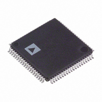
ADV7184BSTZ Analog Devices Inc, ADV7184BSTZ Datasheet - Page 20

ADV7184BSTZ
Manufacturer Part Number
ADV7184BSTZ
Description
IC DECODER VID SDTV MULTI 80LQFP
Manufacturer
Analog Devices Inc
Type
Video Decoderr
Specifications of ADV7184BSTZ
Applications
Projectors, Recorders, Security
Voltage - Supply, Analog
3.15 V ~ 3.45 V
Voltage - Supply, Digital
1.65 V ~ 2 V
Mounting Type
Surface Mount
Package / Case
80-LQFP
Resolution (bits)
10bit
Adc Sample Rate
54MSPS
Power Dissipation Pd
550mW
No. Of Input Channels
12
Supply Voltage Range
1.65V To 2V, 3V To 3.6V
Operating Temperature Range
-40°C To +85°C
Tv /
RoHS Compliant
Input Format
Analogue
Output Format
Digital
Rohs Compliant
Yes
Lead Free Status / RoHS Status
Lead free / RoHS Compliant
Available stocks
Company
Part Number
Manufacturer
Quantity
Price
Company:
Part Number:
ADV7184BSTZ
Manufacturer:
Analog Devices Inc
Quantity:
10 000
ADV7184
FB_INV, Address 0xED [3], Write Only
The interpretation of the polarity of the signal applied to the FB
pin can be changed using FB_INV.
0 (default)—The fast blank pin is active high.
1—The fast blank pin is active low.
Readback of FB Pin Status
FB_STATUS [3:0], Address 0xED [7:4]
FB_STATUS [3:0] is a readback value that provides the system
information on the status of the FB pins, as shown in Table 16.
FB Timing
FB_SP_ADJUST [3:0], Address 0xEF [7:4]
The critical information extracted from the FB signal is the time
at which it switches relative to the input video. Due to small
timing inequalities either on the IC or on the PCB, it may be
necessary to adjust the result by a fraction of one clock cycle.
This is controlled by FB_SP_ADJUST [3:0].
Each LSB of FB_SP_ADJUST [3:0] corresponds to ⅛
clock cycle. Increasing the value is equivalent to adding delay to
the FB signal. The reset value is chosen to produce equalized
channels when the ADV7184 internal antialiasing filters are
enabled and there are only intentional delays on the PCB.
The default value of FB_SP_ADJUST [3:0] is 0100.
Table 16. FB_STATUS Functions
FB_STATUS [3:0]
0
1
2
3
Bit Name
FB_STATUS.0
FB_STATUS.1
FB_STATUS.2
FB_STATUS.3
Description
FB_RISE. A high value indicates that there has been a rising edge on FB since the last
I
FB_FALL. A high value indicates that there has been a falling edge on FB since the last
I
FB_STAT. The value of the FB input pin at the time of the read.
FB_HIGH. A high value indicates that there has been a rising edge on FB since the last
I
th
2
2
2
C read. The value is cleared by an I
C read. The value is cleared by an I
C read. The value is cleared by an I
of an ADC
Rev. A | Page 20 of 112
Alignment of FB Signal
FB_DELAY [3:0], Address 0xF0 [3:0]
In the event of misalignment between the FB input signal and
the other input signals (CVBS and RGB) or unequalized delays
in their processing, it is possible to alter the delay of the FB
signal in 28.63636 MHz clock cycles. (For a finer granularity
delay of the FB signal, refer to the FB_SP_ADJUST [3:0],
Address 0xEF [7:4] section.)
The default value of FB_DELAY [3:0] is 0100.
Color Space Converter Manual Adjust
FB_CSC_MAN, Address 0xEE [7]
As shown in Figure 9, the data from the CVBS and RGB sources
are converted to YPbPr before being combined. For the RGB
source, CSC must be used to perform this conversion. When
SCART support is enabled, the parameters for CSC are
automatically configured for this operation.
If the user wishes to use a different conversion matrix, this
autoconfiguration can be disabled and the CSC can be manually
programmed. For details on this manual configuration, contact an
Analog Devices representative.
0 (default)—The CSC is configured automatically for the RGB-
to-YPrPb conversion.
1—The CSC can be configured manually (not recommended).
2
2
2
C read (this is a self-clearing bit).
C read (this is a self-clearing bit).
C read (this is a self-clearing bit).


