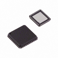
ADV7180BCPZ Analog Devices Inc, ADV7180BCPZ Datasheet - Page 21

ADV7180BCPZ
Manufacturer Part Number
ADV7180BCPZ
Description
IC VIDEO DECODER SDTV 40-LFCSP
Manufacturer
Analog Devices Inc
Type
Video Decoderr
Datasheet
1.ADV7180BSTZ.pdf
(116 pages)
Specifications of ADV7180BCPZ
Design Resources
Low Cost Differential Video Receiver Using ADA4851 Amplifier and ADV7180 Video Decoder (CN0060) Low Cost Video Multiplexer for Video Switching Using ADA4853-2 Op Amp with Disable Function (CN0076)
Applications
Digital Cameras, Mobile Phones, Portable Video
Voltage - Supply, Analog
1.71 V ~ 1.89 V
Voltage - Supply, Digital
1.65 V ~ 2 V
Mounting Type
Surface Mount
Package / Case
40-LFCSP
Resolution (bits)
10bit
Input Format
Analog
Output Format
Digital
Adc Sample Rate
57.27MSPS
Power Dissipation Pd
250mW
No. Of Input Channels
3
Supply Voltage Range
1.71V To 1.89V
Lead Free Status / RoHS Status
Lead free / RoHS Compliant
For Use With
EVAL-ADV7180LQEBZ - BOARD EVALUATION ADV7180EVAL-ADV7180LFEBZ - BOARD EVAL FOR ADV7180 LFCSP
Lead Free Status / RoHS Status
Lead free / RoHS Compliant, Lead free / RoHS Compliant
Available stocks
Company
Part Number
Manufacturer
Quantity
Price
Company:
Part Number:
ADV7180BCPZ
Manufacturer:
ADI
Quantity:
1 470
Company:
Part Number:
ADV7180BCPZ
Manufacturer:
AD
Quantity:
699
Part Number:
ADV7180BCPZ
Manufacturer:
ADI/亚德诺
Quantity:
20 000
Company:
Part Number:
ADV7180BCPZ-REEL
Manufacturer:
HP
Quantity:
600
Company:
Part Number:
ADV7180BCPZ-S
Manufacturer:
MAX
Quantity:
2 230
Part Number:
ADV7180BCPZ-S
Manufacturer:
ADI/亚德诺
Quantity:
20 000
GLOBAL CONTROL REGISTERS
Register control bits listed in this section affect the whole chip.
POWER-SAVING MODES
Power-Down
PDBP, Address 0x0F[2]
The digital supply of the ADV7180 can be shut down by using
the PWRDWN pin or via I
0x0F[5]
pin has the higher priority. The default is to give the pin
(
ADV7180 powered down by default at power-up without the
need for an I
When PDBP is 0 (default), the digital supply power is controlled by
the PWRDWN pin (the PWRDWN bit, 0x0F[5], is disregarded).
When PDBP is 1, the PWRDWN bit has priority (the pin is
disregarded).
PWRDWN, Address 0x0F[5]
When PDBP is set to 1, setting the PWRDWN bit switches the
ADV7180 to a chip-wide power-down mode. The power-down
stops the clock from entering the digital section of the chip,
thereby freezing its operation. No I
down. The PWRDWN bit also affects the analog blocks and
switches them into low current modes. The I
unaffected and remains operational in power-down mode.
The ADV7180 leaves the power-down state if the PWRDWN bit is
set to 0 (via I
PDBP must be set to 1 for the PWRDWN bit to power down
the ADV7180.
When PWRDWN is 0 (default), the chip is operational. When
PWRDWN is 1, the ADV7180 is in a chip-wide power-down mode.
RESET CONTROL
Reset, Chip Reset, Address 0x0F[7]
Setting this bit, which is equivalent to controlling the RESET pin
on the ADV7180, issues a full chip reset. All I
to their default/power-up values. Note that some register bits do
not have a reset value specified. They keep their last written value.
Those bits are marked as having a reset value of x in the register
tables (see
the part immediately starts to acquire the incoming video signal.
1
2
PWRDWN ) priority . This allows the user to have the
For 32-lead, I
For 64-lead, 48-lead, and 40-lead only.
section). PDBP controls whether the I
Table 107
2
2
C is the only power-down option.
2
C) or if the ADV7180 is reset using the RESET pin.
C write.
2
and
2
Table 108
2
C (see the
1
2
C bits are lost during power-
). After the reset sequence,
PWRDWN, Address
2
C registers are reset
2
C interface is
2
C control or the
Rev. F | Page 21 of 116
After setting the reset bit (or initiating a reset via the RESET pin),
the part returns to the default for its primary mode of operation.
All I
self-clearing.
Executing a software reset takes approximately 2 ms. However,
it is recommended to wait 5 ms before any further I
performed.
The I
on the ninth clock cycle when chip reset is implemented (see
the MPU Port Description section).
When the reset bit is 0 (default), operation is normal.
When the reset bit is 1, the reset sequence starts.
GLOBAL PIN CONTROL
Three-State Output Drivers
TOD, Address 0x03[6]
This bit allows the user to three-state the output drivers of the
ADV7180.
Upon setting the TOD bit, the P15 to P0 (P7 to P0 for the 48-lead,
40-lead, and 32-lead devices), HS, VS, FIELD (VS/FIELD pin for
the 48-lead, 40-lead, and 32-lead LFCSP), and SFL pins are
three-stated.
The timing pins (HS, VS, FIELD) can be forced active via the
TIM_OE bit. For more information on three-state control, see
the Three-State LLC Driver and the Timing Signals Output
Enable sections.
Individual drive strength controls are provided via the
DR_STR_x bits.
When TOD is 0 (default), the output drivers are enabled.
When TOD is 1, the output drivers are three-stated.
Three-State LLC Driver
TRI_LLC, Address 0x1D[7]
This bit allows the output drivers for the LLC pin of the
ADV7180 to be three-stated. For more information on three-
state control, refer to the Three-State Output Drivers and the
Timing Signals Output Enable sections.
Individual drive strength controls are provided via the
DR_STR_x bits.
When TRI_LLC is 0 (default), the LLC pin drivers work
according to the DR_STR_C[1:0] setting (pin enabled).
When TRI_LLC is 1, the LLC pin drivers are three-stated.
2
C bits are loaded with their default values, making this bit
2
C master controller receives a no acknowledge condition
ADV7180
2
C writes are


