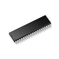
AT89C55-24PI Atmel, AT89C55-24PI Datasheet - Page 4

AT89C55-24PI
Manufacturer Part Number
AT89C55-24PI
Description
Microcontrollers (MCU) 80C31 w/20k
Manufacturer
Atmel
Datasheet
1.AT89C55-24JI.pdf
(24 pages)
Specifications of AT89C55-24PI
Data Bus Width
8 bit
Program Memory Type
Flash
Program Memory Size
20 KB
Data Ram Size
256 B
Interface Type
UART
Maximum Clock Frequency
24 MHz
Number Of Programmable I/os
32
Number Of Timers
3 x 16 bit
Operating Supply Voltage
4 V to 5.5 V
Maximum Operating Temperature
+ 85 C
Mounting Style
Through Hole
Package / Case
PDIP-40
Minimum Operating Temperature
- 40 C
Lead Free Status / Rohs Status
No
Available stocks
Company
Part Number
Manufacturer
Quantity
Price
Part Number:
AT89C55-24PI
Manufacturer:
ATMEL/爱特梅尔
Quantity:
20 000
4-172
ALE/PROG
Address Latch Enable is an output pulse for latching the
low byte of the address during accesses to external mem-
ory. This pin is also the program pulse input (PROG) dur-
ing Flash programming.
In normal operation, ALE is emitted at a constant rate of
1/6 the oscillator frequency and may be used for external
timing or clocking purposes. Note, however, that one ALE
pulse is skipped during each access to external data mem-
ory.
If desired, ALE operation can be disabled by setting bit 0 of
SFR location 8EH. With the bit set, ALE is active only dur-
ing a MOVX or MOVC instruction. Otherwise, the pin is
weakly pulled high. Setting the ALE-disable bit has no
effect if the microcontroller is in external execution mode.
PSEN
Program Store Enable is the read strobe to external pro-
gram memory.
When the AT89C55 is executing code from external pro-
gram memory, PSEN is activated twice each machine
cycle, except that two PSEN activations are skipped during
each access to external data memory.
EA/V
External Access Enable. EA must be strapped to GND in
order to enable the device to fetch code from external pro-
gram memory locations starting at 0000H up to FFFFH.
Note, however, that if lock bit 1 is programmed, EA will be
internally latched on reset.
EA should be strapped to V
tions.
This pin also receives the 12-volt programming enable volt-
age (V
XTAL1
Input to the inverting oscillator amplifier and input to the
internal clock operating circuit.
XTAL2
Output from the inverting oscillator amplifier.
Special Function Registers
A map of the on-chip memory area called the Special
Function Register (SFR) space is shown in Table 1.
Note that not all of the addresses are occupied, and unoc-
cupied addresses may not be implemented on the chip.
Read accesses to these addresses will in general return
random data, and write accesses will have an indetermi-
nate effect.
PP
PP
) during 12-volt Flash programming.
AT89C55
CC
for internal program execu-
User software should not write 1s to these unlisted loca-
tions, since they may be used in future products to invoke
new features. In that case, the reset or inactive values of
the new bits will always be 0.
Timer 2 Registers Control and status bits are contained in
registers T2CON (shown in Table 2) and T2MOD (shown
in Table 4) for Timer 2. The register pair (RCAP2H,
RCAP2L) are the Capture/Reload registers for Timer 2 in
16 bit capture mode or 16-bit auto-reload mode.
Interrupt Registers The individual interrupt enable bits are
in the IE register. Two priorities can be set for each of the
six interrupt sources in the IP register.
Data Memory
The AT89C55 implements 256-bytes of on-chip RAM. The
upper 128-bytes occupy a parallel address space to the
Special Function Registers. That means the upper 128-
bytes have the same addresses as the SFR space but are
physically separate from SFR space.
When an instruction accesses an internal location above
address 7FH, the address mode used in the instruction
specifies whether the CPU accesses the upper 128-bytes
of RAM or the SFR space. Instructions that use direct
addressing access SFR space.
For example, the following direct addressing instruction
accesses the SFR at location 0A0H (which is P2).
Instructions that use indirect addressing access the upper
128-bytes of RAM. For example, the following indirect
addressing instruction, where R0 contains 0A0H, accesses
the data byte at address 0A0H, rather than P2 (whose
address is 0A0H).
Note that stack operations are examples of indirect
addressing, so the upper 128-bytes of data RAM are avail-
able as stack space.
MOV 0A0H, #data
MOV @R0, #data


